


Guía de reparación de la tablero hash de Innosilicon Miner [EN]
Document Type: Maintenance Plan
Contents of this booklet: Mainly describes how to troubleshoot various faults of the T1.T2 hash board and how to use the test to accurately locate.
Scope: applicable to all T1 production, after‑sales, and outsourcing maintenance sites
1. Maintenance platform requirements:
1. Constant temperature soldering iron ( 350 Degree‑‑ 400 Degrees), the pointed soldering iron tip is used for soldering small patches such as chip resistors and capacitors. Skilled mastery.
2. The hot air cylinder is used for chip disassembly and soldering. Be careful not to heat it for a long time to avoid PCB foaming.
3. DC stabilized power supply (output 12V, 20A), used for the test and measurement of the hash board.
4. Fluke 15b+ multimeter, tweezers, Debug, G7 maintenance special control board, oscilloscope.
5. Flux solder paste, washing water and absolute alcohol; washing water is used to clean up the solder residue and appearance after repair.
6. Tin planting fixture, planting tin steel mesh, solder paste; when replacing a new chip, you must plant the chip with tin.
7. The thermal conductive glue is black, high temperature, gray low temperature used for re-attaching the heat sink after maintenance.
2. Requirements on Maintenance Operations:
1. The maintenance personnel must have certain electronic knowledge, more than one year of maintenance experience, and master QFN package welding technology.
2. After repairing, the hash board must be tested twice and confirmed as OK before it can pass!
3. Pay attention to the operation method when replacing the chip. After replacing any accessories, the PCB board is not obviously deformed, and the replaced parts and the surrounding area shall be checked for whether there is open and short circuit.
4. Determine the maintenance station object and the corresponding test software parameters and test fixtures.
5. Check whether the tools and jigs can work normally.
3. Principle and structure:
● Principle overview
1. T1 is composed of 21 voltage domains in series, each voltage domain has 3 chips, and the whole board has 63 T1558 chips.
2. The T1558 clock is two 12M crystal oscillators, which are transmitted in series from the first chip to the 30th, and 31 to the last chip.
3. There is an independent small heat sink on the back of each chip of T1. The small heat sink on the back is fixed on the back of the IC with thermal glue after the initial test of the board. Repair and replace the chip after passing the test, you need to evenly apply black thermal conductive glue on the IC surface and heat it to fix it.
● Analysis of key points:
The following figure shows the SPI trend and voltage domain of the PCB board and the chip sequence bit number.
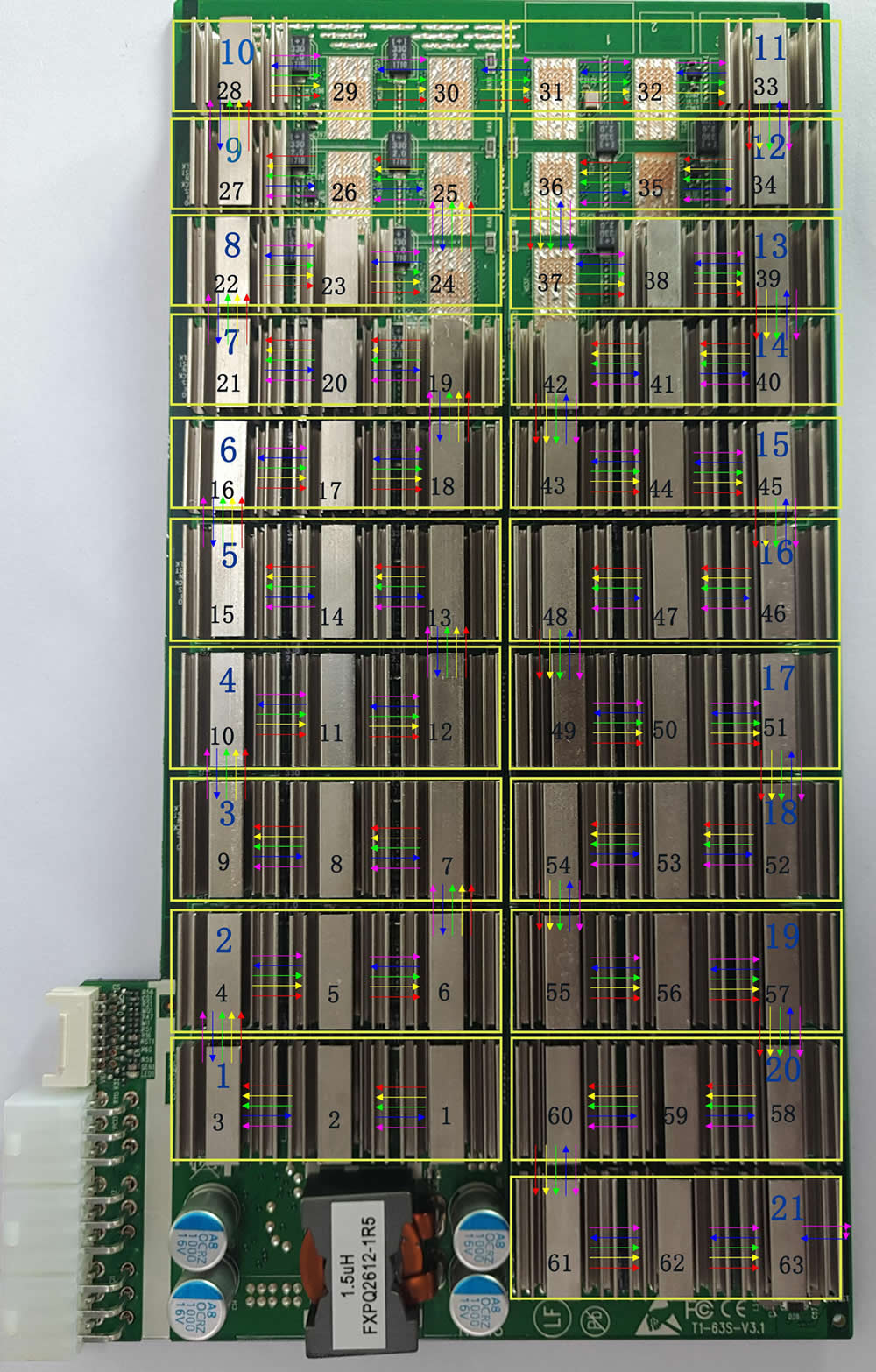
figure 1
Test whether the SPI waveform of the error‑reporting chip is normal.
1. Each yellow box in the figure is a voltage domain, a total of twenty one Voltage domains, each voltage domain is on average 0.42V.
2. The black numbers represent the order and bit number of the chip.
3. The red arrow in the figure shows CLK Signal direction.
The yellow arrow shows the direction of the SCK signal;
The green arrow shows the direction of the CS signal;
The blue arrow shows the direction of the DI signal;
The purple arrow shows the direction of the DO signal.
4. There is between every two chips 1‑7 Test point 1 for CLK Signal; test point 2 for RST Signal; test point 3 for EN Signal; test point 4 for SCK Signal; test point 5 for CS Signal; test point 6 for DI Signal; test point 7 for DO signal.
DI signal flow direction, from No. 63 chip to 1 Return the chip number, and then return to the control board;
DO signal flow direction, by 1 No. chip pulls low level toward 63; not plugged in IO Line, standby 0V , When calculating 0.3 Pulse signal around.
The RST signal flows in from the control board, and then by 1 Chip to 63 No. chip transmission.
2.2 The figure below shows the key circuits on the front of the T1 hash board.
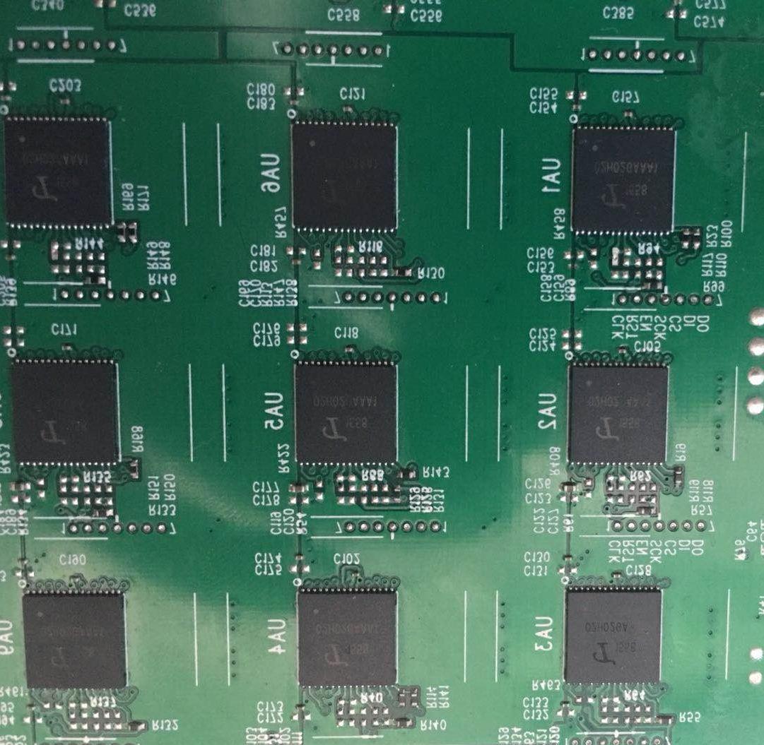
figure 2
1). Test points between each chip (as shown in the figure after zooming in): Figure 2
Figure 2. When repairing test points between chips, the test points between test chips are the most direct way to locate faults. The arrangement of the test points of the T1 arithmetic board is: CLK, RST.EN, SCK, CS, DI, DO signals.
Figure 1. Signal trend
2) Voltage domain: The whole board has 21 voltage domains, and each voltage domain has 3 chips. The three chips in the same voltage domain are powered in parallel, and then connected in series with other voltage domains after being connected in parallel. The circuit structure is shown in Figure 4 below:
Principle analysis of voltage domain single chip (see Figure 3 below)
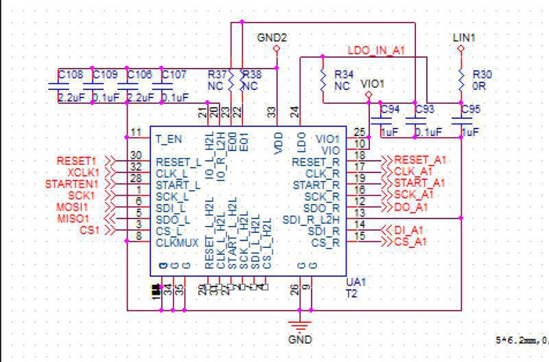
Figure 3
● The above are the functions of each pin of the T1558 chip.
During maintenance, 14 test points before and after the chip are mainly tested (seven points before and after the chip: CLK, RST, EN, SCK, CS, DI, DO); DCDC voltage output 8.82V; boost voltage 11V, LDO--1.8 V etc.
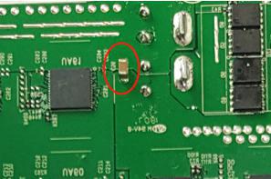
The two ends of the C56 capacitor on the left are the total DCDC output voltage, which should be about 8.82V
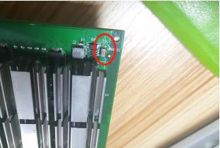
On the left, both ends of the C57 capacitor are the boost voltage, which should be about 11V

Figure 6. BM1558 circuit diagram
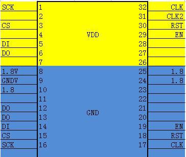
Figure 7. BM1760 chip pins
CLK: 0.9V provided by Y1 12M crystal oscillator;
DO: From the first chip to the last chip provided by the control board, the signal can be measured with an oscilloscope;
DI: Return from the last chip to the first chip, the signal can be measured with an oscilloscope;
SCK: When the control board provides about 0.12V for calculation, the abnormal or low voltage will cause the calculation board to be abnormal or the calculation power is low;
EN: 1.8V Provided by the control board;
CS: Provided by the control board;
RST: 1.8V . Provided by the control board, each time the test key is pressed, a low‑level reset signal will be output again.
When the above‑mentioned test point status and voltage are abnormal, please estimate the fault point based on the circuit before and after the test point.
It can be seen from the chart above:
CLK signal: by the chip 32 Or 31‑pin in, 17‑pin out, when connected across the voltage domain, by 5 Foot out through 100NF The capacitor is connected to the input to the next chip twenty three foot.
DO signal: enter from pin 6 of the chip, 12 Foot out;
DI signal: returned by the chip from pin 5, output from pin 13 or 14;
CS signal: input from pin 3 of the chip and output from pin 15;
RST signal: Input from chip 30 pins, output from 118 pins.
Test the signal voltage of each chip, LDO‑1.8OV
CORE: 0.8V When this voltage is abnormal, it is usually the chip of the voltage domain CORE Short circuit
LDO‑1.8O: 1.8V When this voltage is abnormal, the chip LDO‑1.8O Short circuit or open circuit
3) Judging the operating status of the hash board, the hash rate of the chip, and the temperature sensitivity based on the information in the printing window of the manufacturing tool.
3.3 IO Interface Definition
IO is composed of 2X7 pitch 2.0 PHSD 90 degree in‑line double row.
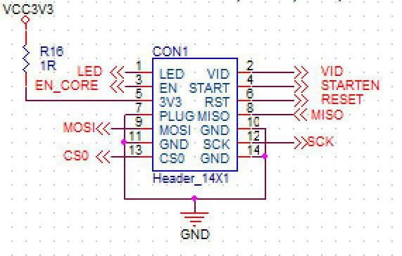
The pin definitions are shown in Figure 8 below:
As shown in FIG:
1 pin is LED
2 pin for VIDD
10, 14 pin: for GND .
3 pin are EN
4 pin for STAR
7 pin is PLUG
12 pin for SCK
13 pin are CS
8.9 pin (DI, EO)
6 pin ( RST ): is the reset signal 3.3V Terminal, after being divided by resistors, it becomes 1.8V RST Reset signal.
5 pin ( 3V3 ): is the hash board 3.3V Power supply, the 3.3V Provided by the control board, mainly for PIC Provide working voltage.
Figure 8. IO Definition of each pin
TX_IN voltage is 1.8V
RST_IN voltage is 1.8V
4. Routine maintenance process:
● Reference steps:
1. Routine inspection: First, perform visual inspection on the arithmetic board to be repaired to observe whether there is any displacement, deformation, or scorching of the small heat sink? If any, you must deal with it first; if the small heat sink is displaced, remove it first, wash off the original glue, and re‑adhesive after the repair is passed.
Secondly, after the visual inspection is no problem, the impedance of each voltage domain can be tested first to detect whether there is a short circuit or an open circuit. If you find out, you must deal with it first.
Thirdly, check whether the voltages in each voltage domain reach 0.4v, and the voltage difference between the voltage domains must not exceed 0.05. If the voltage in a voltage domain is too high or too low, the circuits in the adjacent voltage domain generally have abnormal phenomena, and it needs to find the reason first.
2. After the routine detection is no problem (generally, the short‑circuit detection of the routine detection is necessary, so as not to burn the chip or other materials due to the short circuit when the power is turned on), you can Use DEBUG connection for chip detection, and judge and locate according to the detection result.
3. According to the display results of the test and detection, starting from the vicinity of the faulty chip, check the chip test points (CLK, RST, EN, SCK, CS, DI, DO); DCDC voltage output 8.82V; boost voltage 11V, LDO‑‑ 1.8V etc.
4. Then according to the signal flow direction, except for DI signals, the signals are transmitted in the reverse direction (chips 6 to 1). Several of the signals CLK, RST, EN, SCK, CS, DO are forward transmission (1-63), and abnormalities are found through the power supply sequence the point of failure.
5. When locating the faulty chip, the chip needs to be welded again. The method is to add flux around the chip (preferably no-clean flux), heat the solder joints of the chip pins to a dissolved state, move gently up and down, left and right to press the chip; prompting the chip pins and pads Re-melt and collect tin. In order to achieve the effect of tinning again. If the fault remains the same after re-soldering, you can directly replace the chip.
6. The repaired arithmetic board must be tested twice or more during testing. Two test times before and after: for the first time, after the replacement of parts is completed, the hash board needs to be cooled down, and after passing the test, put it aside first. For the second time, after a few minutes wait for the arithmetic board to cool down completely, perform the test again. Although the time for the two tests is a few minutes, this does not affect the work. Put the repaired board aside, continue to repair the second board, wait for the second board to be repaired and set it aside to cool down, and then test the first board. In this way, the time is just staggered, and the total time is not delayed.
7. The repaired board. It is necessary to classify the faults and make records of the type, location, reason, etc. of the replacement components. For feedback back to production and after‑sales, Research and development.
8. After recording, install it into a complete miner for formal aging.
5. Failure types:
1. The impedance of each voltage domain is unbalanced; when the impedance of certain voltage domains deviates from the normal value, it indicates that there are parts in the abnormal voltage domain that have open circuits and short circuits. It is most likely to be caused by general chips. But there are three chips in each voltage domain, and often only one has a problem when it fails. The method of finding out the problem chip can detect and compare the abnormal point through the test point to ground impedance of each chip. If you encounter a short-circuit phenomenon, you can first remove the heat sink on the chip with the same voltage, and then observe whether the chip pins are connected to the solder. If the short-circuit point cannot be found in the appearance, the short-circuit point can be found according to the resistance method or the current interception method.
2. Voltage imbalance in the voltage domain; When the voltage of some voltage domains is too high or too low, it is generally because of abnormal voltage domains or adjacent voltage domains that there are abnormal signals, resulting in abnormal working status of the next or next voltage domain and voltage imbalance . The abnormal point can be found only by detecting the signal and voltage of each test point. Individually, it is necessary to find out the abnormal point by comparing the impedance of each test point.
Observe the appearance, measure the impedance, measure the voltage, and check the voltage and power supply of each test point. The test locates the chip according to the test information, first re-soldering, and re-soldering is invalid. The fault type is recorded and tested for more than two times. Ok can be considered as repaired, and then related aging.
Pay special attention to the fact that the CLK signal and RST Signal, these two abnormalities are most likely to cause voltage imbalance.
3. Lack of chips: The lack of chips means that the test box fails to detect all 63 chips, often only as many as the actual number of chips. However, the actual missing (undetected) abnormal chip is not in the displayed position. At this time, it is necessary to accurately locate the abnormal chip through testing. The location method can use TX cut-off to send out the way to find the location of the abnormal chip. It is to connect the TX signal of a certain chip to the ground. For example, after outputting the TX signal of the 50th chip to the ground of the voltage domain, theoretically if all the previous chips are normal, 50 chips should be detected in the test box? If 50 chips are not detected, the abnormality is before the 50th chip; if 50 chips are detected, the abnormality is after the 50th chip. By analogy, use the dichotomy to find the location of the abnormal chip.
4. Broken chain:
A broken chain is similar to lack of chips, but in a broken chain, not all chips that cannot be found are abnormal, but all the chips after the abnormal chip are invalid due to a certain chip abnormality. For example, a chip itself can work, but it will not forward other chip information; at this time, the entire signal chain will come to an abrupt end, and lose a large part of it, which is called broken chain. Generally the broken chain can be displayed by the test box. For example, when the test box detects the chips, only 14 chips are detected. If the number of preset chips is not detected in the test box, it will not run, so it will only display how many chips are detected, at this time, according to the displayed number "14", the problem can be found by detecting the voltage and impedance of each test point before and after the 14th chip.
5. Not running:
No running means that the test box cannot detect the chip information of the hash board, but displays NO hash board; this phenomenon is the most common and the fault range involved is also wide.
1) Non‑operation caused by abnormal voltage in a certain voltage domain; the problem can be found by measuring the voltage of each voltage domain.
2) The abnormality caused by a certain chip abnormality can be found by measuring the signal of each test point.
CLK signal: the signal is generated by 1 No. chip output to 63 No. chip, but the current version has only two crystal oscillators, Y1(1‑30) X1(31‑63) of which as long as there is an abnormal signal clk Yes, all the following signals will be abnormal, search in order according to the signal transmission direction.
DO signal: This signal is caused by 1 , 2 , 3 ,,,,, 63 No. chip, when a certain point of the dichotomy is abnormal, it can be detected forward.
DI signal: This signal is returned by No. 63.60, 59, 58, and 1, and the cause of the fault is confirmed through the chip signal direction. This signal is the highest priority if the T1 operation board is not running, and the signal is searched first.
RST signal: 1.8V ; After the arithmetic board is powered on and the 14P signal is plugged in, this signal will change from 01 , 02 ,,,,,, 0 63 The direction of the transmission to the last chip.
3) A certain chip VDD It can be caused by measuring whether the potential difference of each voltage domain is normal. Under normal circumstances, when the VDD voltage is 0.42, the normal voltage of each test point in other voltage domains is also 0.42 to ensure the balance between the voltage domains.
4) of a certain chip VDD1V8 Abnormal voltages Determine whether a certain VDD1V8 voltage is normal by measuring the test points of each voltage. Generally, the LDO voltage determines the voltage of each test point. When the LDO voltage is 1.8V, the normal voltage of each test point in other voltage domains is also 1.8. V
5. Low hash rate:
Low hash rate can be divided into:
1) During the test, received Nonce Insufficient, lack of hash rate and show bad phenomena. This phenomenon can be judged by seeing the number of nonce returned by each chip directly through the serial port printing information. Generally, the chip with the returned nonce number lower than the set value should be trouble‑shooted, and the non‑welding and external causes can be directly replaced. .
2) When the test fixture was tested, the hash rate was low after the whole miner was installed. Most of this situation is related to the heat dissipation conditions of the chip, and special attention should be paid to the glue used for the small heat sink of each chip and the ventilation performance of the whole miner. Another reason is that the voltage of a certain chip is critical. After the whole miner is installed, the difference between the 12V power supply and the power supply during the test causes the test calculation power to deviate from the running calculation power. You can use the test box to test after turning it down, and adjust it slightly. After the 12V output of the voltage DC adjustable power supply, perform the test again and find out the voltage domain with the lowest number of returned nonces.
6. A certain chip NG:
Refers to when the test is passed, the test serial port information shows that the returned nonce of a certain chip is insufficient or zero. In addition to eliminating the problem of false soldering and peripheral components, you can Replace the chip directly.
● Maintenance instructions:
1. During maintenance, the maintenance personnel must be familiar with the function and flow direction of each test point, the normal voltage value and the ground impedance value.
2. You must be familiar with chip soldering to avoid blistering and deformation of the PCB or damage to the pins.
3. T1558 chip package, 16 pins on both sides of the chip. The polarity and coordinates must be aligned during welding and they must not be misaligned.
4. When replacing the chip, the thermally conductive fixing glue around the chip must be cleaned to prevent the chip from being damaged by the hanging or poor heat dissipation when the IC is soldered.
عملاؤنا الكرام:
مرحباً! تبدأ عطلة عيد العمال الصيني من 1 إلى 5 مايو 2026 (بتوقيت غرينتش +8). سيتم تعليق خدمات الشحن الدولي خلال هذه العطلة. ستقوم شركتنا بتعليق الشحنات بعد ظهر يوم 30 أبريل 2026، وستُستأنف عمليات الشحن من المستودعات يوم 6 مايو (بتوقيت غرينتش +8). نعتذر بشدة عن أي إزعاج قد يسببه هذا الأمر. شكرًا لتفهمكم ودعمكم.
مع خالص التقدير،
ZEUS MINING CO., LTD.