


Guía de reparación de la tablero hash de Antminer S15 [EN]
Editor: Li Yan
Doc. Version: 2019.07.02
Doc. Category: Maintenance Guide
Content of This Doc.: mainly about the fault checking and hashboard tester pinpointing of Antminer S15.
I. Maintenance Platform Requirements
1. Thermostat soldering iron at 300-350 degrees Celsius, pointed solder tip for small patches like r-c.
2. Heat gun for chip disassembly and soldering, no long-time heating in case of PCB blistering (the soldering temperature shall be 260±2 degrees Celsius).
3. APW8 power supply with 16.32V-20.04V output to test the hash board.
4. Fluke 15b+ Multimeter, tweezer, V9-1.2 hash board tester (oscilloscope preferred).
5. Scaling powder, cleaning water and anhydrous alcohol; cleaning water is used to clean the residue and appearance after maintenance.
6. Tin grinder, tin stencils, and tin cream (low temperature OM550); implant tin for chips upon renewals.
7. Heat-conducting Glue, black (6223), to glue cooling fin after maintenance.
II. Maintenance Requirements
1. Maintenance technician in possession of good electronics knowledge, 1 year+ experience and sound mastery of QFN encapsulation and soldering techniques.
2. Check more than two times after maintenance and the result of each time is OK!
3. Watch out for the techniques used, make sure of no obvious PCB deformation after changing any fittings, check for missing/open circuit/short circuit on parts.
4. Check the maintenance target and corresponding test software parameter and hash board tester.
5. Check whether tools and testers can work properly.
III. Principle and Structure
● Principle Introduction
1. Antminer S15 has 12 voltage domains connected in series, each domain has 5 BM1391, and the entire board has 60 BM1391 chips.
2. BM1391 chip has 3 built-in small voltage domains which are connected in series.
3. BM1391 has 12 voltage domains; S15 has 25M monocrystal oscillator on the clock, connecting in series and passing on from the 1st chip to the last chip.
4. S15 has independent small cooling fins on the front and back of each chip. The cooling fin on the front is SMT paster and the cooling fin on the back is fixed on the back of IC by heat-conducting glue after initial test. Upon completion of every maintenance, it has to be fixed by black heat-conducting glue (evenly distributed) on the back of IC.
5. Power supply of S15 is APW8, the output of it is regulated by the control panel. The normal voltage is 220V, there will be no output of APW8 without a control panel to regulate the voltage.
Note:
In the process of maintenance, when changing board fittings or chip, in order to avoid the damage to PCB and chip caused by the heat from the blower gun, cooling fins near the malfunctioning part and the cooling fin on the back of PCB need to be removed firstly before conducting fitting changes.
PCB has test points on both sides, use the front one during maintenance in production before fitting cooling fin on the front; in product maintenance (after-sales maintenance), cooling fins are on both sides of PCB, locate fault through test points of PCB, and use specially made long and thin pen-shape meter to probe into the gaps of cooling fin for test; because the SMT small cooling fins connect the ground of each voltage domain, watch out the insulation of pen-shape meter, to avoid short circuit caused by pen-shape meter.
● Key Point Analysis:
2.1 S15 Signal Flow(Fig1)
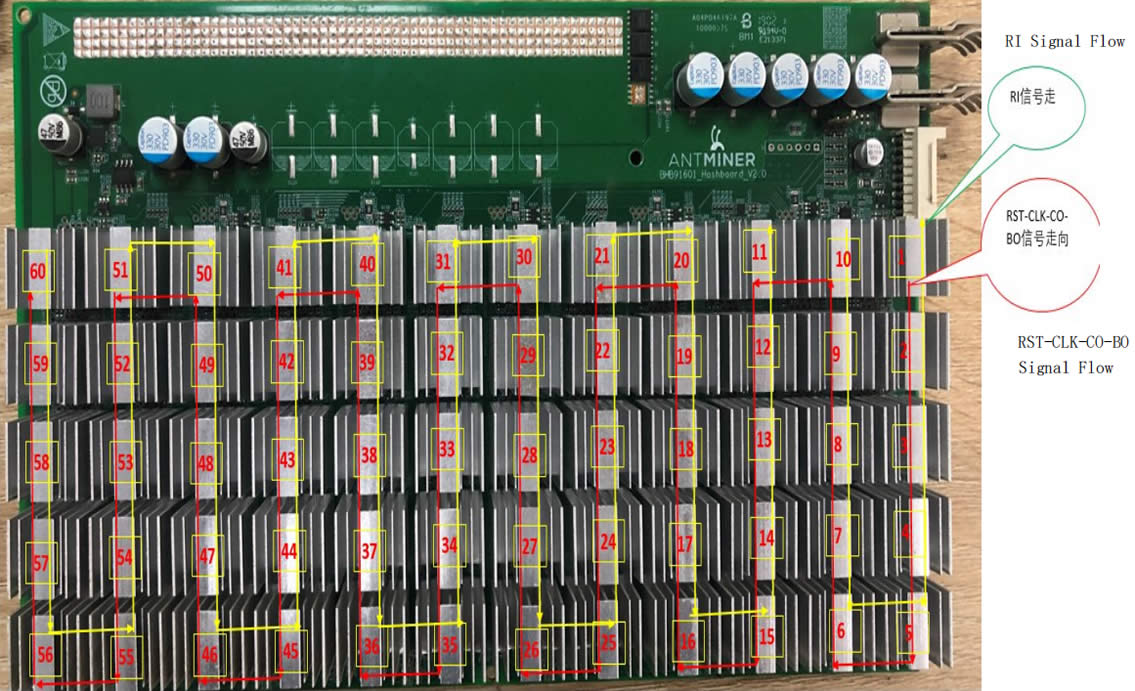
Fig 1. S15 Signal Flow
Red is CLK signal flow, produced by Y1 25M crystal oscillator, transmits from No. 1 chip to No. 60 chip; in standby and computing, both the votalges are 0.9±0.1V.
Red is TX (CI, CO) signal flow, IO mouth pin 7 in, transmits from No. 00 to No. 62; the voltage is 0V when IO signaling wire is not plugged, and the voltage is 1.8V in computing.
Yellow is RX (RI, RO) signal flow, returns from No. 60 to No. 00, and then returns to control panel from IO mouth pin 8; the voltage is 0V when IO signaling wire is not plugged, and the voltage is also 1.8V in computing.
Red is B (BI, BO) signal flow, lowers electrical level from No. 00 to No. 60; the voltage is 0V when IO signaling wire is not plugged or in standby, and the singal impluse is about 0 in computing.
Red is RST singal flow, IO mouth pin 3 in, transmits from No. 00 to No. 62 chip; 0V when IO signaling wire is not plugged or in standby, and 1.8V in computing
2.2 The key circuit on the front of the hash board (Figure 2)
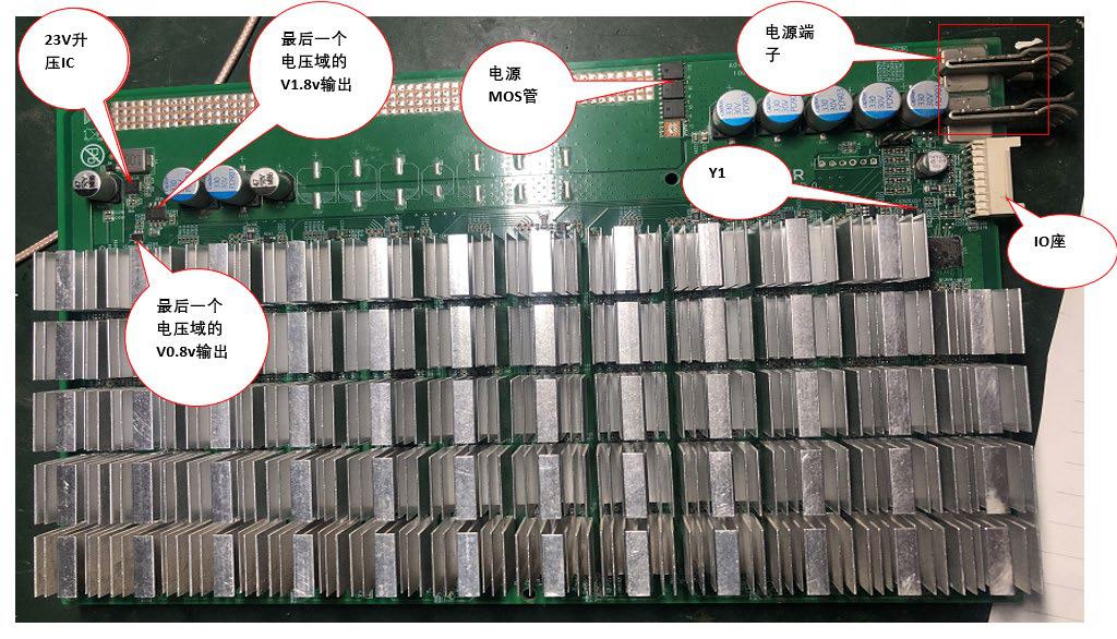
Figure 2 Key circuits on the front of hash board S15
2.2.1 Test points between chips (Figure 3)
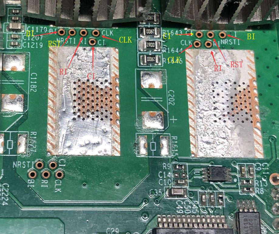
Figure 3 Test points between chips
At the time of maintenance, the test points between the test chips are the most direct fault location methods.
The arrangement of the test points on hash board S15 is as shown in the left figure.
2.2.2 Voltage domain
There are 12 voltage domains on the entire board, each with 5 chips. The 5 chips in the same voltage domain are powered by the associated power supply, and then connected with other voltage domains in series. The circuit structure is shown in Figure 4 below:
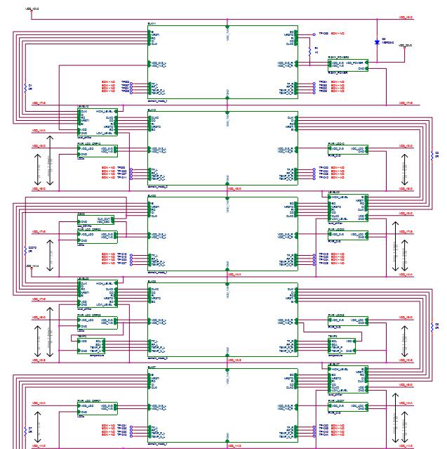
Figure 4 Key circuit on the front of hash board S15
Principle analysis of single chip in the voltage domain (see Figure 5 below):
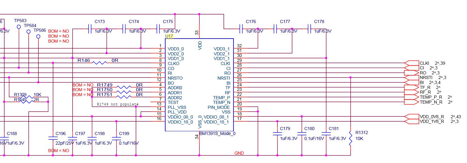
Figure 5 BM1391 circuit diagram
The above is the function of each pin of chip BM1391.
At the time of overhaul, the 10 tests before and after the main test chip (five before and five after the chip: CLK, CO, RI, BO, RST).
Test method:
① When the jig is not tested, APW8 only outputs 12V to the jig’s control board, with no output of 19.2V;
② When the jig starts testing, APW8 will output 19.2V voltage to the power supply of the control board. During the test, the voltage at each test point of the jig is as follows:
CLK: 0.9V
CO: 1.6-1.8V, when the jig just sends WORK, since the CO is negative, the DC level will be lowered, and the instantaneous voltage is about 1.5V.
RI: 1.6-1.8V, when computing, if the voltage is abnormal or too low, the hash board will be abnormal or the hashrate will be zero.
BO: 0V. When not computing, it is 0V; when computing, there will be a pulse jitter between 0.1-0V.
RST: 1.8V. Each time the test button of the jig is pressed, a reset signal will be re-output.
When the above-mentioned test point status or voltage is abnormal, please estimate the fault point based on the circuit before and after the test point. It can be seen from the above list:
CLK signal: input from pin 29 of the chip, output from pin 8, when connected across the voltage domain, output from pin 8 and connected to pin 29 of the next chip through the 0 ohm resistor.
TX signal: input from pin 28 of the chip, and output from pin 9;
RX signal: returned from pin 10 of the chip, output from 27 pin;
BO signal: input from pin 25 of the chip, output from pin 12;
RST signal: input from pin 26 of the chip and output from pin 11.
3. IO port
IO consists of 2X9 pitch 2.0 PHSD in 90-degree in-line dual row.
The definition of each pin is shown in Figure 6 below:
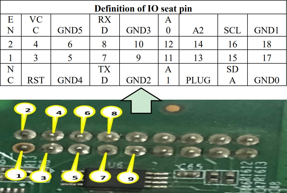

Figure 6 Definition of each pin of IO port
As shown in the figure above:
Pins 5.6.17.18: GND.
Pins 15.16 (SDA, SCL): It is the I2C bus of DC-DC PIC, connecting the communication between the control board and the PIC. The control board can read and write the data of the PIC through it to control the running status of the hash board and connect to U6-EPROOM. This IC mainly stores PCB, BOM and chip, and sweeps information.
Pin 13 (PLUG0): It is the identification signal of the hash board. This signal is pulled from the 10K resistor to 3.3V on the hash board. Therefore, when the IO signal is inserted, the pin should be at high level.
Pins 11.12.14 (A2, A1, A0): PIC address signal. Connect to U6-EPROOM.
Pins 7.8 (TXD, RXD): the channel for hashrate at the end 3.3 of the hash board. After being divided by the resistor, it becomes signals TX (CO) and RX (RI). The level of the IO port pin is 3.3V. After being divided by the resistor, it becomes 1.8V.
Pin 3 (RST): Reset signal on the 3.3V terminal, and becomes a 1.8V RST reset signal after being divided by the resistor.
Pin 4 (D3V3): Supply power 3.3V to the hash board, which is provided by the control board, mainly to provide working voltage to the PIC.
4. 23V boost circuit
It is responsible for boosting DC-DC (19.2v) to 23V. The principle is to increase the voltage from 19.2V to 23V through the U7 switching power supply. The switching signal produced by U7 is the energy storage inductor through L4, and the D4 charges and discharges C73-C75 through boost rectifier diode, and then filtered by EC26 to obtain 23V at EC26 positive electrode. The 23V voltage is output to U170, the u170 outputs 1.8V and then outputs 0.8V through u171, as shown in Figure 7.
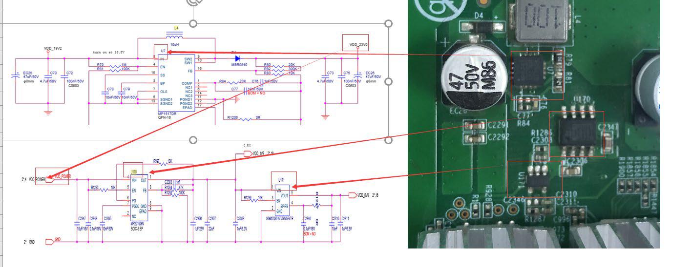
Figure 7 23V boost circuit
5. DC-PIC
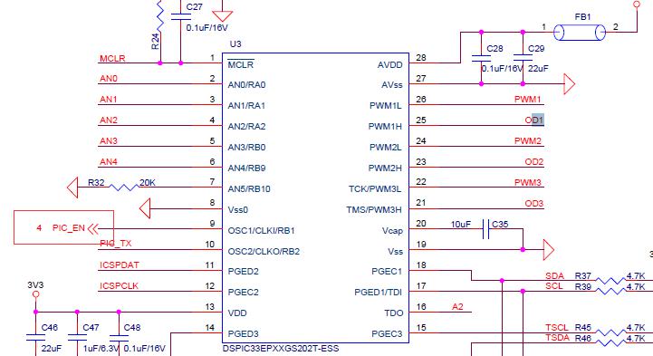
It consists of PIC16(L)F1704 (Figure 8, Figure 9).
A device that stores the frequency information and voltage value of the hash board chip, and also controls the DC-DC output voltage of the hash board.
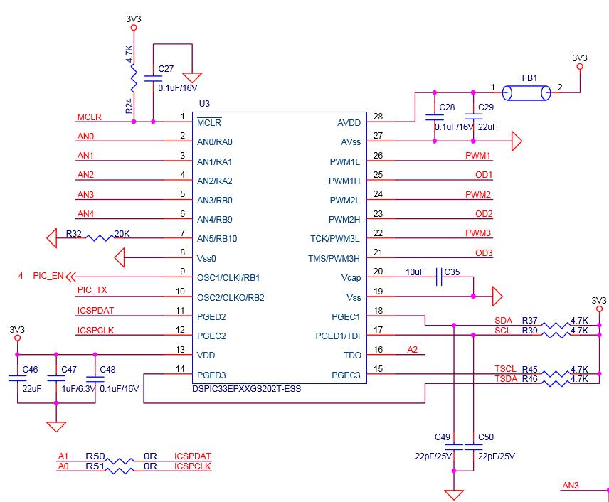
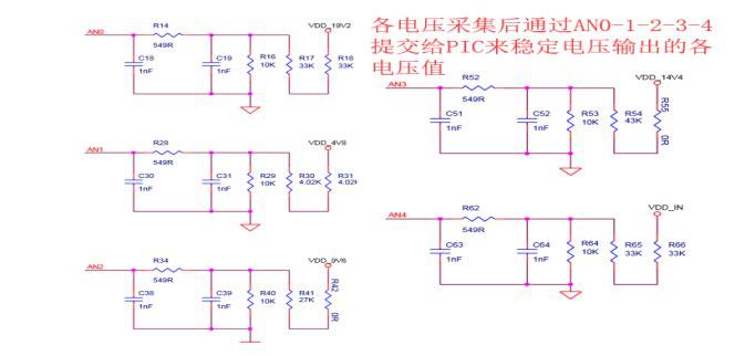
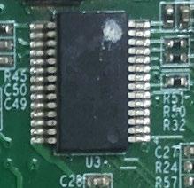
Figure 9 PIC schematic diagram
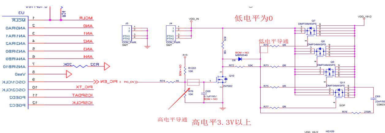
Figure 10 PIC circuit
6. DC-DC circuit
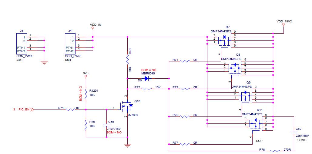
It consists of 2N7002 and CMOS tubes (Figure 11, Figure 12).

Figure 11 DC-DC schematic diagram
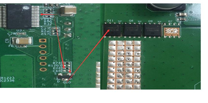
Figure 12 DC-DC physical diagram
When the circuit is not working: PIC-EN9 pin output low level and lowers Q10's pin 1 to make Q10 non-conducting, and causes high level of pin 4 of Q7-8-9-11MOS tube to cut MOS, and there is no voltage output.
7. 25M LCK
It consists of a Y 25MHZ passive crystal oscillator and 12pF (Figure 13 and Figure 14).
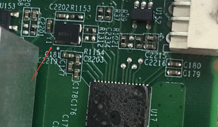
Figure 13 25M LCK circuit

Figure 14 25M LCK principle
When normal, the voltage at the two ends of R1154 is about 1V±0.1.
8. Temperature sensing circuit
There are 4 temperature senses: one is TEMP (PCB), which is composed of sensor IC; the other is TEMP (CHIP), which is the built-in temperature sensor group (BM1391 21st, 22nd pins). After collecting the parameters of these two temperature sensors, they are finally returned by RI to the FPGA of the control board through the 23rd and 24th pins of BM1391. The principle is shown in Figure 15:


IV. Examples for single board test troubleshooting
1. Single board jig test ASIC=0
Failure analysis:
1.1 Whether the jig cable and the hash board are in good contact.
1.2 If it is the S15 hash board, J4-J5 should have a voltage of 18.36V when testing the jig.
1.3 When testing the jig, measure whether there is voltage between the 12 voltage domains.
1.3.1 If there is no voltage in the voltage domain, it is necessary to see whether the normal working voltage of pin 4 of Q7, Q8, Q9, Q11 is 0V. If it is at high level, then see whether pin 1 of Q10 is high or equal to 3.3v, if Q10 does not have a voltage of 3.3V, then the U3-PIC loses firmware or has no power.

PIC schematic diagram
19.2V output control circuit
1.3.2 If the power supply is normal and there is voltage in the voltage domain, then it is necessary to measure the RI signal of the chip to see if the RI signal has a voltage of 1.8V. When measuring the RI signal, it should start from the test point of the last chip. If there is voltage in the last chip, the 36th chip can be measured for whether there is RI -1.8v; when the chip has no RI output voltage, the 1.8V power supply of this chip is measured first, if there is no 1.8V power, then it is necessary to check the 1.8V power supply circuit. The 1.8V obtains 3.2V to supply the LDO pin 1 after being dividing by the voltage domain. The LDO pin 5 outputs 1.8V, (each voltage domain has one chip power supply -1.8V LDO), if there is no output, it should be the problem of this LDO, if 1.8V is normal, the ground resistance of the test point can be measured after the power is off and compared with the OK board to see if there is resistance abnormality. If the resistance is normal, and there is no problem in soldering, the chip should be defective. (Re-solder the removed chip to a good board to verify it. If there is no RI signal, the chip is defective, replace a new chip).

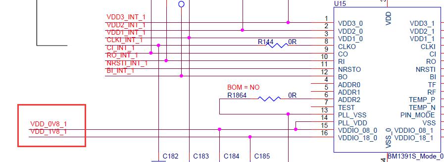
1.8V power supply circuit
1.3.3 The method described in this article is applicable to the fault caused by some hashrate chips or LDO damage of S15. The insufficiency of ASIC caused by short circuit or poor soldering may also use this method for location.
Step 1: First check the appearance of the faulty hash board for whether the cooling fin is complete, whether the circuit board is burnt, whether the MOS tube is burnt out, and whether the capacitor is burnt out, etc.
Step 2: Measure the resistance from the LDO output to this LDO GND without powering. The pin installation of the LDO is shown in Figure 1, which measures the resistance from Pin5 to Pin2.
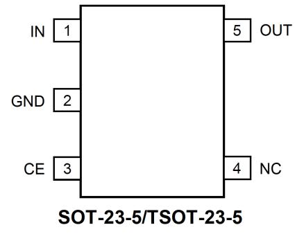
Figure 1 LDO pin installation
As measured in Figure 2, 0.868K is the resistance of normal 1.8V LDO, and 41.4 ohms is the resistance of normal 0.8V LDO. The third figure is a bad indication. Under normal circumstances, the LDO has been burned, and the corresponding domain also has power chip damage. In this case, the LDO should be replaced and the resistance should be tested again. If the resistance is normal or the resistance is large, the next step can be operated.
 Table 1 LDO list
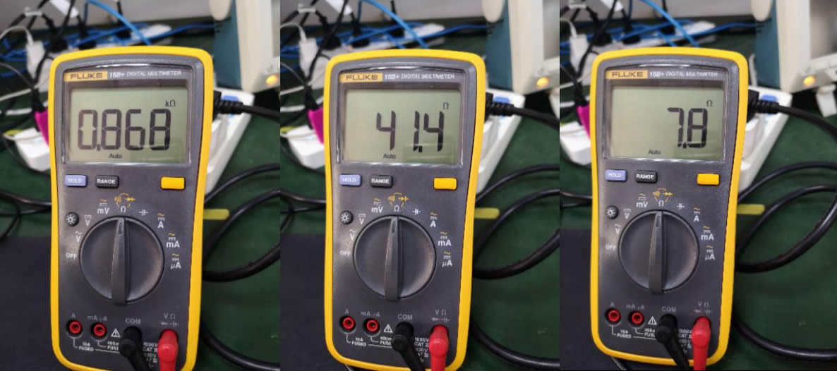 Figure 2 Multimeter reading
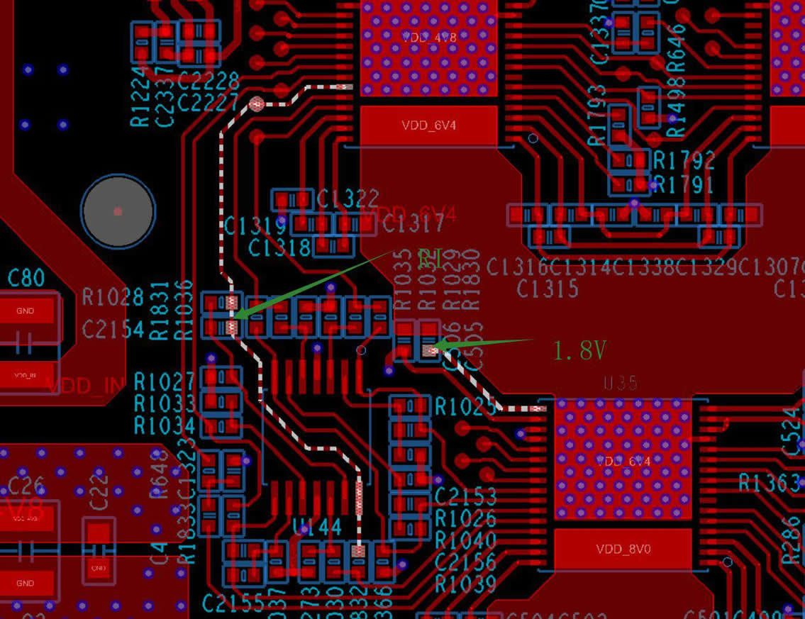
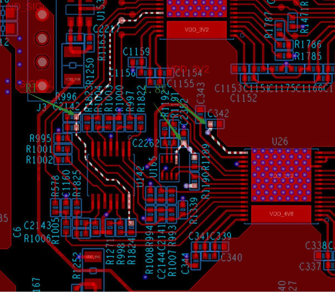
Step 3: Power on and short connect RI to the corresponding 1.8V for single board search chip test.
In the case of LDO damage, after replacing the LDO, the check can be started from this domain. When the RI is short connected to 1.8V, the number of chips recovered should be the number of all chips before the short connection point. If the number is correct, continue to look backwards. If it is zero, the chip before the test point has a problem and needs to be replaced.
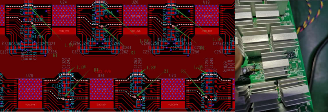
The way RI is short connected to 1.8V to check the number of chips is divided into two types: cross-domain chip and intra-domain chip. As shown in Figure 3, red is a cross-domain chip. It is recommended to check each red cross-domain chip to quickly determine the domain, and then locate the intra-domain chip. (The second and third cooling fins of the problem domain can be easily checked for problem checking).
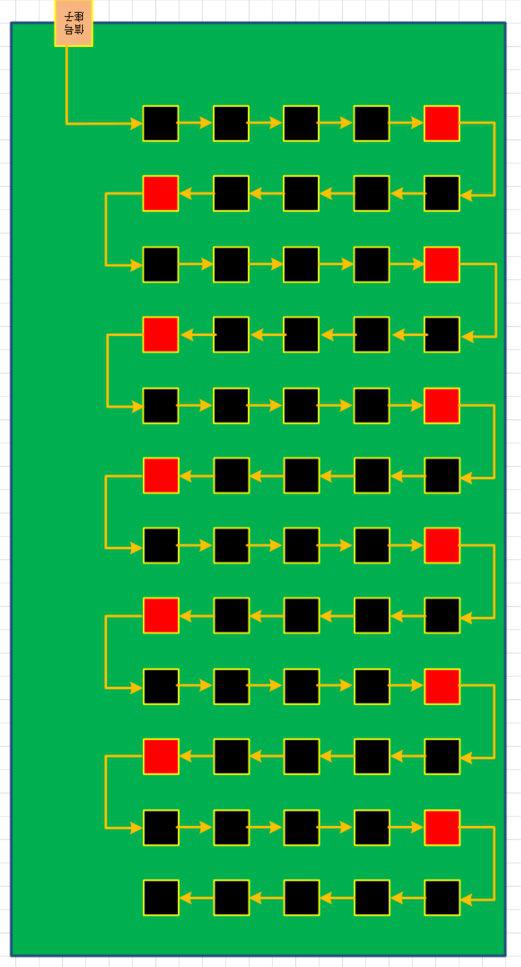
Figure 3 Chip layout
Here's how to short connect through PCB:
① Cross-domain short connection
Short connect the RI to 1.8V, run the single board jig to find the chip:
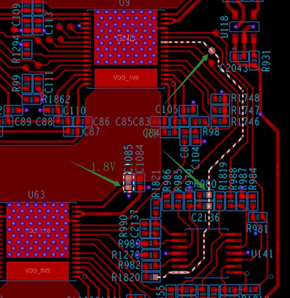
② Intra-domain short connection
Note that there are two types of RI locations in the domain, as shown in the following figure:
2. Single board jig test ASIC = 23
Failure analysis:
2.1 Single board test can find 23 chips, and can determine that the RI signal is normal; if the 24th chip cannot be found, we will directly measure the 23rd chip’s U33 CLK-RST-CO voltage to see if the power supply is normal, if CLK has no 0.8V voltage, see the power supply circuit of CLK.
2.2 CLK circuit analysis: If CLK does not have 0.8V, first check whether the 0.8V power supply in the bad chip voltage domain is normal, 0.8V power supply circuit is obtained by voltage divider in the voltage domain as the 1.8V power supply mode; pin 5 outputs 0.8V, as for the maintenance method, you can refer to the 1.8V maintenance method (note that S15 has 2 chips among the 6 chips in each domain that outputs 0.8V LDO power supply, and every LDO supplies to 3 chips).


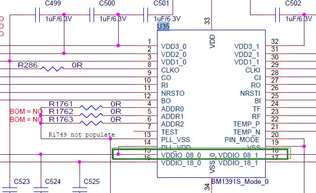
0.8v power supply schematic diagram
If the 0.8V power supply circuit does not output 0.8V, then see if the 0.8V LDO power supply has a supply voltage of about 3.2V. If it has, see if the LDO has pseudo soldering or short circuit. If there is a 0.8V output, check the ground resistance of the chip; if the resistance is correct, it should be a faulty chip.
V. Detection and determination of the status of the entire miner
Whether the operation of the entire miner is normal mainly depends on whether the miner can start normally, and whether the hashrate is normal. If the hashrate is normal, first enter the miner IP to see the following parameters:
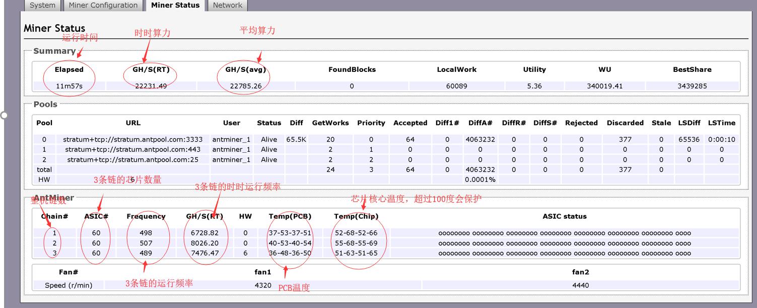
miner test interface diagram
1. Whether 3 chains are detected. If it is not detected enough, see whether the cable is off or the cable is not plugged in, if the chain is still insufficient after upgrading the cable, you can conduct a single board test on the hash board with insufficient chain to see if it is OK.
1.1 The hash board is basically OK, it can be determined that the problem lies in the control board, and it can be excluded by the substitution method.
1.2 If the hash board tests ASIC0, then repair according to the single board maintenance method.
2. Check whether the number of chips is enough, if the number of chips is not enough, you can directly enter the IP-LOG to see whether the chain can detect the chip, and then repair according to the single chip.
3. See whether the running frequency of the 3 chains is normal, the frequency determines the hashrate; one chain’s hashrate = frequency x chip core number 256x chip number 60; if this theoretical hashrate cannot be reached, it proves that there are a lot of bad cores in the chip of this chain. If you want to improve the hashrate, you can enter IP-LOG to see if the chip's frequency is low and replace that chip.
4. Generally, in the case of normal operation of a miner, the temperature of the PCB and chip of the 3 chains is between 25 and 95 degrees. If the temperature of a chain is only below 25 degrees, it proves that the hashboard of the chain does not work, and it needs to test the single board to see if the board is normal. If it is higher than 95 degrees, it proves that the heat dissipation is not good, and it needs to check the fan running condition and ventilation, and also pay attention to whether the cooling fin is off.
5. If you can't see any data after entering IP, but only see the interface as shown below, you need to enter the IPlog to see what information is printed in the log, and repair the miner according to the information; there may be a network outage, or other problem.
6. When the entire miner is repaired, it is repaired according to the mining condition and LOG. Directly replace the piece considered to have problem by a good component and judge.
VI. The principle and structure of the control board
1. Structure of the control board
Name and distribution of control board components
2. Circuit diagram of the network port line
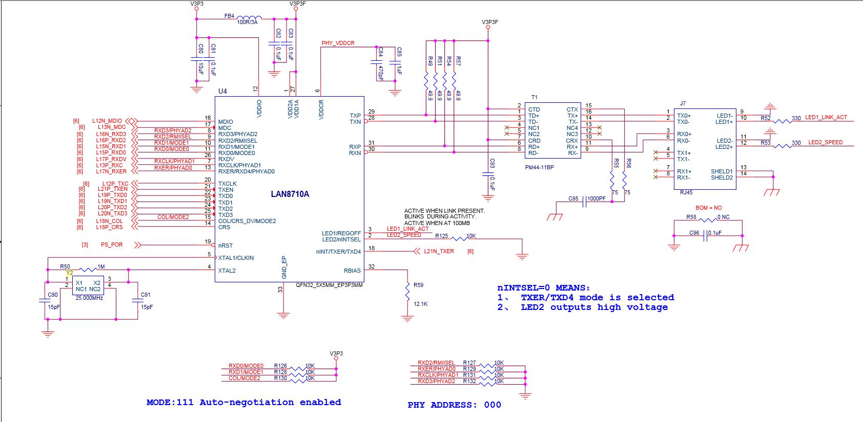
Cannot recognize IP (that is, no network is found): First look at the appearance of the bad board for there there is pseudo soldering with material drop, if the
appearance is normal, find an OK network cable (the network cable being used, plug into the J7 network interface) to see if it can find the IP, if you still can't
find the IP, take an OK control board, and compare the resistance with the bad control board; first measure from pins J7 1, 2, 3, 6, then from T1 1, 2,3,6,7,8,
you can also connect 2 control boards to 12V, compare and measure the voltage of each point, U4 signal is directly connected to the CPU, in general, T1 is
more likely to be bad.
3. Power supply voltage regulating circuit
In the voltage regulating circuit, the CPU directly reads the signal voltage collected by the PIC of hashboard to directly control the APW8 power supply from the J11 output signal, and adjust the APW8 output to stabilize the required voltage.
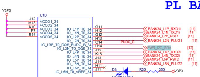
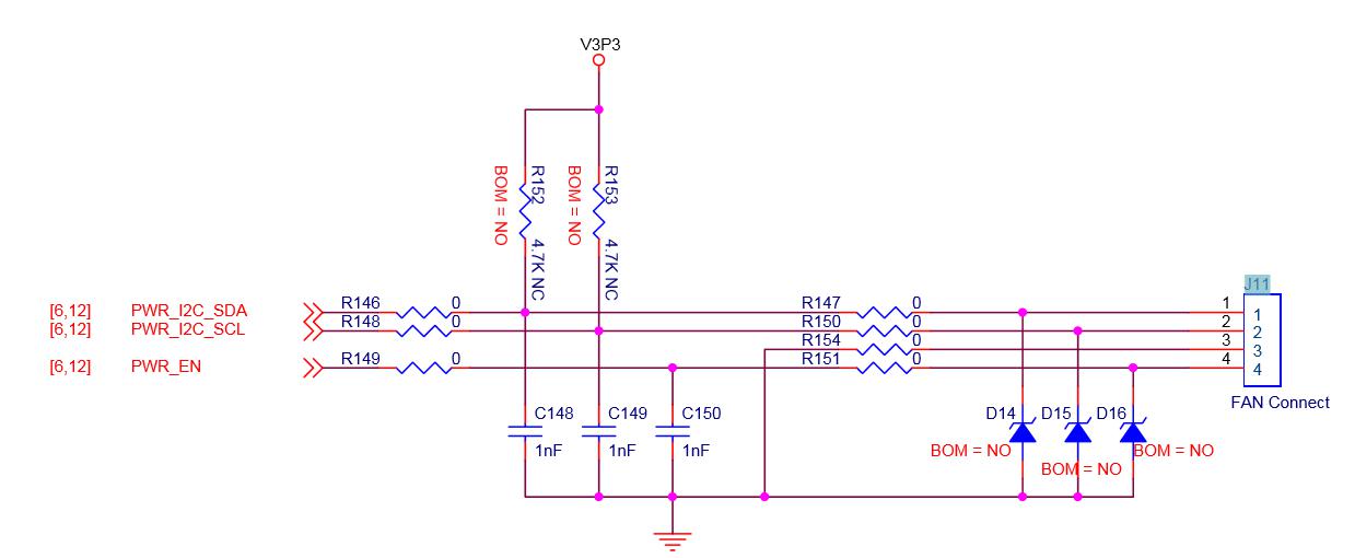
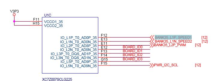

The IO block circuit is directly connected to the CPU. If there is no problem in appearance and soldering, it is basically a CPU problem.
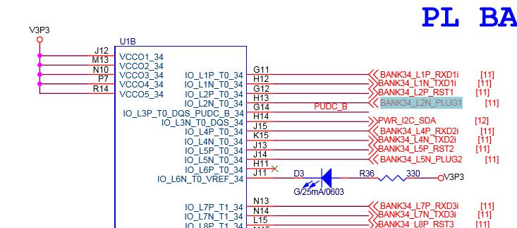
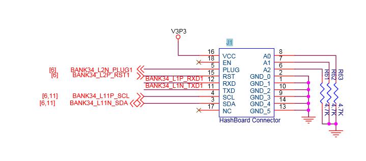
4. Small voltage conversion output circuit

عملاؤنا الكرام:
مرحباً! تبدأ عطلة عيد العمال الصيني من 1 إلى 5 مايو 2026 (بتوقيت غرينتش +8). سيتم تعليق خدمات الشحن الدولي خلال هذه العطلة. ستقوم شركتنا بتعليق الشحنات بعد ظهر يوم 30 أبريل 2026، وستُستأنف عمليات الشحن من المستودعات يوم 6 مايو (بتوقيت غرينتش +8). نعتذر بشدة عن أي إزعاج قد يسببه هذا الأمر. شكرًا لتفهمكم ودعمكم.
مع خالص التقدير،
ZEUS MINING CO., LTD.