Contents of this brochure:The main story S9 Troubleshooting of various faults in the Operation board,how to use the test box for accurate positioning.
Range:Applies to All S9 Production, After-sale, Outside the coordination repair site.
Ⅰ. Maintenance Platform Requirements
1. Thermostatic soldering Irons(350-400°C ), tip for solder chip resistor capacitors and other small patches.
2. Hot air cylinder for chip disassembly welding, be careful not to heat up for a long time lest PCB Foaming
3. APW3++ Power Supply(Output 12V、133A Max), used for test measurement of the Operation board.
4. Fluke 15b+ Multimeter, Sub-camera, S9 Test Jigs(Conditional configurable Oscilloscope).
5. Flux solder paste, washing plate water plus anhydrous alcohol; Wash plate water is used to clean and repair the residue and appearance of welding. Tin-Planting fixture, tin-sik Steel mesh, Solder Paste; When replacing a new chip, you have to plant tin on the chip.
6. Thermal conductive adhesive black(3461), Re-glue the heatsink after servicing.
7. Tools for repairing the S11 miner are indispensable. But when your miner fails, it may also be necessary to replace some damaged parts, such as the cooling fan of the miner, the chip heat sink on the hash board, and the Antminer power cable.
Ⅱ. Job requirement Items
1. Maintenance personnel must have some knowledge of electronics, more than one year of maintenance experience, and master QFN packaging welding technology.
2. After maintenance, the hash board must be tested two times and confirmed as OK before it can pass!
3. Pay attention to the operation method when replacing the chip. After replacing any accessory, the PCB is not obvious deformation of the plate, check the replacement parts and the surrounding there are few open circuit problems.
4. Determine the maintenance station object and the corresponding test software parameters and test fixture.
5. Check whether the tools and fixtures can work normally.
Ⅲ. Principle and Structure
1.Principle Overview
1.1 S9 is composed of 21 voltage domains connected in series. There are 3 BM1387 chips in each voltage domain, and there are 63 BM1387 chips in the whole board.
1.2 The BM1387 has a built-in buck diode with a step-down diode function that is determined by the chip's designated pin.
1.3 S9 is 21 voltage domains (S5+ is 16 voltage domains, S7 54 chip is 18 voltage domains, S7 45 is 15 voltage domains);
1.4 S9 clock is 25M single crystal oscillator, connected in series by the first chip is passed to the last chip.
1.5 There are independent small heat sinks on the front and back of each chip. The small heat sink on the front side is the SMT patch. The small heat sink on the back side is fixed on the back of the IC by the thermal adhesive after the initial measurement. After the repaired and replaced chip passes the test, it is necessary to evenly apply black thermally conductive adhesive on the IC surface and heat and fix it.
Note:
In the maintenance process, in order to reduce the damage of the high temperature of the air gun to the PCB and the chip when replacing the components of the electric board or the chip, it is necessary to first place the small heat sink near the faulty component and the PCB board.
After the small heat sink on the back is removed, replace it.
The PCB board has test points anyway, during the maintenance of the production, the front test points can be used when the heat sink is not attached to the front of the PCB; the finished product repair (after-sales maintenance), due to the front and back of the PCB covered with heat sinks, it is necessary to locate the fault through the test points of the PCB. The special slender pen can be used to probe the gap of the heat sink for measurement, but since the SMT small heat sink is connected to the ground of each voltage domain, when measuring, pay attention to the insulation of the test leads to avoid short circuit caused by the test leads.
2.Key point Analysis
2.1 The following figure is S9 Schematic diagram of signal board signal direction:
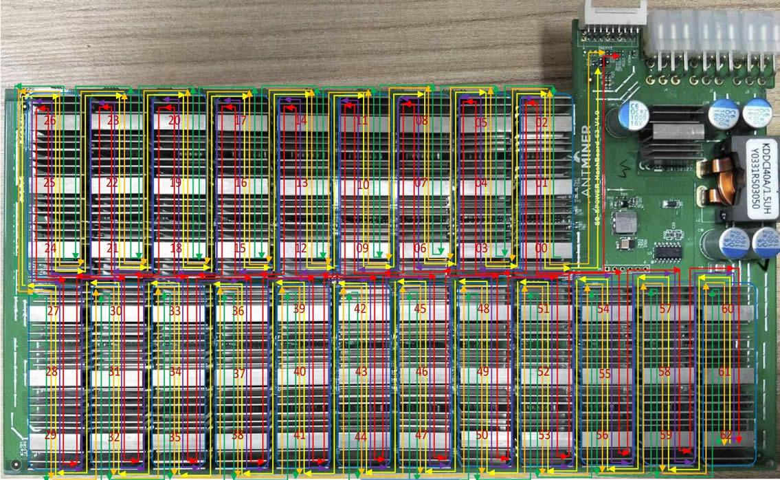
1. Signal direction
>Green line is the flow direction of the CLK signal, from the signal flow direction, from the signal flow direction, generated by the Y1 25M crystal oscillator, from the generation, from the 00 chip to the chip to the 62 chip transfer chip transmission; standby; standby and operation, electricity and operation, electricity When the operation is performed.
>Orange line is the signal flow direction of TX (CI, CO) signal. It enters from IO port 1 and then enters, and then transmits from chip No. 00 to chip to chip 62. When the voltage is line is not inserted, the voltage is 0. The voltage at the time of operation is 1.8V..
>Yellow line is the RX (RI, RO) signal flow direction, and the chip returns from the chip No. 62 to the chip No. 00, and then returns to the control return board from the IO port 12 pin. When the IO signal is not inserted, the voltage is the voltage at the time of 1.8V. When the operation is performed, the voltage is also 1.8V when the operation is performed.
>Purple line for B(BI、BO)Signal Flow,由 00 Number chip toward 62 Pull Low Level;Not plugged in. I Line, Standby time is 0V,When the operation is 0.3 Around the pulse signal. Purple is B (BI, BO) signal flow, ) signal flow, from 00 chip to chip to 62 low level; no low level; no low level; no low level; no IO line It is 0V during standby, and is a pulse signal of about 0.3 at the time of calculation. Pulse signal.
>Red line is the flow direction of RST signal, signal flow direction, signal flow direction, from IO port 15 foot, then from, then from, then from 00 chip to 62 chip transfer chip transmission chip transmission; no IO signal, standby It is 0V during standby, and is calculated during operation. It is 1.8V when calculating.
2.2 Figure 3 shows the key circuits on the front of the S9 hash board.

figure 2. inter-chip test points
1) test points between each chip (After zooming in the image below): figure 2
During maintenance, the test point between the test chip is the most straight the fault location mode of the connection. S9 Operational Board test pilot Row listed as:
Upper Row 9 Sequencing of voltage domains: RST, B0, RI(RX), C0(TX), CLK Signal.
Bottom row 12 The order in which the voltage domains are arranged in turn: CLK, CO(TX), RI(RX), BO,RST.

figure 3. S9 Key circuits on the front of the Operation board
2) voltage Domain:Full board has 21 Voltage domain, Each voltage has three chips. In the same voltage domain. 3 A chip to power the associated power supply, The correlation is then concatenated with the other voltage domains. Circuit structure such as The following figure 4 is shown:


figure 4. S9 Key circuits on the front of the Operation board
Note that:
Because the version of the S9 hash board is not exactly the same, the LDO-1.8V power supply of the early voltage domains is powered by a separate peripheral LOD power supply chip for each of the three voltage domains. The later version is changed to the internal chip. Power supply (BM1387 chip with 2.5 V input, 1.8V output LDO supply circuit), except for the last six voltage domains, which are powered by 14V boost and LDO externally, all other chips provide LDO1.8V power supply, while PLL -0.8V is obtained by dividing the first chip LDO -1.8V in each voltage domain by a voltage divider resistor (late version).
Principle analysis of single chip in voltage domain (Figure 5 Figure 6 below):

Figure 5. BM1387 Circuit diagram

Figure 6. BM1387 Chip Pin
Signal Description

● Above is BM1387 Chip each pin function.
During overhaul, before and after the main test chip 10 A test(Five before and after the chip: CLK, CO, Re, BO, RST); CORE Voltage; LDO-1.8V, PLL-0.8V, DC-DC Output and boost 14V Voltage.
Detection method:
1) Do not plug IO line, plug only 12V: DC-DC output is around 9V, the boost output voltage is around 14V. Test points must have LCK= 0.9V, RI =1.8V voltage,other test voltages is 0;
2) Plug in IO, when you do not press the test key, DC-DC No voltage output with boost, after pressing the test key, PIC start working, at this time DC-DC output PIC, PIC tool test program sets the voltage, rises with the working voltage. Test program set the voltage, boost up with the work. With the output of the system WORK, return after operation NONC. At this point the normal voltage of each test point should be:
CLK: 0.9 in CO:1.6-1.8 V, test tool sends work, CO Because it's negative. So the DC level will be pulled low, Instantaneous voltage is 1.5 V Around.
RI: 1.6-1.8 V, when operating, an abnormal or too low voltage can cause the operator board to be abnormal or force 0 the situation.
BO: When no operation is 0V, when operating will have 0.1-0.3 V between the pulse beats.
RST: 1.8 in. The reset signal is re-exported every time the test key of the fixture is pressed.
When the above test point state, voltage anomaly,please infer the point of failure based on the front and rear circuitry of the test point.
● Visible from list above:
CLK Signal: By the Chip pin 24 (XIN), pin 6 out (CLK0), When connecting across voltage domains, by pin 6 out through 100NF Capacitance connection input to next chip pin 24.
TX Signal: Chip pin 27 in (CI_A), Pin 5 out (CO);
RX Signal: Chip pin 4 back (RI), Pin 28 output (RO);
BO Signal: Chip pin 30 in (BI_A), Pin 2 output (BO);
RST Signal: Chip Pin 32 in (NRST_A), Pin 1 output (NRSTO).
Figure below 7 is shown: The signal voltage of each chip can be measured, CORE Voltage LDO-1.8 or, LDO-1.8I, PLL-0.8, LDO-2.5I
Equal voltage:
CORE: 0.4---When this voltage is abnormal, generally the voltage domain of the chip CORE Short circuit
LDO-1.8 or: 1.8---When this voltage is abnormal, the chip LDO-1.8 or Or LDO-1.8I Short or open circuit
LDO-1.8I: 1.8---When this voltage is abnormal, the chip LDO-1.8 or Or LDO-1.8I Short or open circuit
PLL-0.8: 0.8 in---When this voltage is abnormal, the voltage domain has a chip PLL-08 Power supply short-circuit, or LDO-1.8 Abnormal.
LDO-2.5I: 2.5---When this voltage is abnormal, the chip LDO-2.5I Short or open circuit.

Figure 7. Chip peripheral test point and each voltage
3) According to the information on the diagnostics tool, the operational state of the Operation board, the chip arithmetic ability and the temperature sense are judged.
3. IO Port: IO by 2X9 pitch 2.0 PHSD 90 the degree of straight-in double-row composition. The individual pins are defined as the following figure 8 is shown:

Figure 8. IO Pin definition for each port
As shown in the figure above:
1, 2, 9, 10, 13, 14: GND
3, 4 (SDA, SCL): DC-DC PIC I2C Bus, Connect the Control Panel to PIC of communication, The control board can read and write through it PIC Data, Control the operating state of its operational board.
5 (PLUG0): Identifying signals for the operating board,This signal is pulled by the operator board. 10K Resistance to 3.3 in,So plug it in. I Signal when,the foot should be to high level.
6, 7, 8 (A2、A1、A0): PIC Address signal.
11,12 (Txd、RXD): For the arithmetic board 3.3 End of the counting force of the channel, after being divided by a resistor, it becomes TX(CO), RX(RI) Signal, I Port pin End ping du for 3.3v, after the voltage is divided by the resistor, become a 1.8v.
15 (RST): To reset the signal 3.3v, After being divided by the resistor, it becomes 1.8v in RST Reset Signal.
16 (D3V3): For the arithmetic board 3.3v Power supply, 3.3v Provided by the Control Panel, Mainly to the PIC provides operating voltage.
Figure 9, Figure 10 are shown as IO Voltage and distribution of each pin before and after the pressure is divided.

Figure 9. I Each voltage of the signal

Figure 10. IO The signal is divided into piezoelectric
4. 14V Boost circuit:
Responsible for the DC-DC(8.3 — 9.2 V)Boost to 14V, the principle is through U110 (RT8537) The switching power supply will boost 9v to 14 V, the switching signal produced by U110 passes the output switch signal through L1 The switching signal produced by U110 passes the output switch signal through L1 for storage. can inductance, inductor, a boost rectifier diode D100 and then C954 to charge and discharge, whereby the discharge, to thereby obtain a positive electrode C954 of 14 V。 As shown in figure 11Figure 12 is shown:

Figure 11. 14V Boost schematic diagram

Figure 12. 14V Boost PCB
Need to be aware of: An abnormally high voltage rise in the boost circuit can lead to the calculation board finally 6 Voltage domain. LDO Damage, also easily lead to chip damage. While the boost voltage the exception is mostly U110, R812, R811 Oxidation-induced.
5. DC-PIC: PIC16 (L) F1704 Composition As shown in figure 13 and Figure 14:
A device that stores the frequency information and voltage values of an operational board chip, It also allows control of the operational DC-DC Output voltage.

Figure 13. PIC Schematic diagram

Figure 14. PIC
PIC is running, every minute, we need to control the heartbeat signal. If not, With heartbeat information, PIC will work for one minute and then shut down.
PIC pin 1 is VDD 3.3V, 14 is GND, pins 9 and 10 are connected to the I2C bus of the IO port to the control board, pins 5, 6, and 7 are PIC addresses; pin 4 is PIC3 .3V; pin 8 is PIC.
FB output, control DC-DC voltage; 11 pin is EN signal of PIC output, control DC-DC working status.
6. DC-DC Circuit: LM27402SQ and CMOS tube TPHR9003NL Composition Figure 15 below and Figure 16 is shown:

Figure 15. DC-DC Schematic diagram

Figure 16. DC-DC Circuit
LM27402SQ Voltage Regulator Generation PWM Switching signals drive up and down bridges (Two pairs CMOS), and through L2 Inductor Energy Storage, Again by C19, C20 Filtering.
LM27402SQ Main function Pin
Pin 7: 12V Power supply
Pin 9, 17: GND
Pin 2: FB Feedback Connection PIC Voltage determined by pin 8 of Pic to decide.
Pin 10: Vdd
Pin 13: Bootstrap capacitance 10v +
Pin 16: Pulse
Pin 12: Switching signal
Pin 11: Lower Bridge Drive
Pin 14: Upper Bridge Drive
DC-DC When the voltage is abnormal, First check through the fixture printing information to view PIC is the voltage value DC-DC is the output voltage one to; If there is a disagreement between, Please change first LM27402SQ The small capacitance around;
If DC-DC No output, Please check R13, R14 Voltages 1v on both sides - R11 Voltage 12V, PIC Whether the work is abnormal, PIC Whether the control panel can be accepted properly I2C Signal.
DC-DC Output voltage Standard:
14T Operation Board: 8.3 V-8.6 V
13.5T Operation Board: 8.4 V-8.7 v
13T Operation Board: 8.4 V-8.9 v
12.5T Operation Board: 8.5 V 9.1 V
12T the following operational board: 8.6-9.2 V
If this range is exceeded, please check DC-DC Circuit.
7. 25M Clock and 25MHZ Passive crystal oscillator and 12pF Composition: As shown in figure 17 and Figure 18 Normal time, R70 Each end voltage is 1v Around.

Figure 17. 25M LCK Circuit

Figure 18. 25M LCK Principle
8. 1.8V-LDO by 1.8 VLDO SPX5205M5_L_1_8 Composition
Figure 19 and Figure 20 is shown: SPX5205M5 pin 1, 3 as input, pin 5 for 1.8V Output;
It is important to note that: S9 of the Operation board LDO There are two modes of power supply operation. One is that each voltage domain of an operational board is an external LDO, SPX5205M5, Responsible for each voltage domain's 3 A chip. LDO; The other is only the last 6 Voltage domain Setting External LDO, The other voltages are built-in by the chip. LDO Provide yourself; BM1387 Chips are Ready-built LDO Power supply Circuit, 由 BM1387 的14(LDO-25I) pin input, 10 脚(LDO-18th) Output, And each chip has a separate LDO, Non-interference. At last 6 Voltage domain. LDO-25I The power supply is from 14V Boost circuit; Other voltage-domain LDO-25I is by the rear 6 Voltage domain. CORE Voltage superposition gain(6 *. 04V = 2.4 Around).
PLL-08 Voltage by LOD-1.8 It is obtained by two resistance voltage divider.

Figure 19. 25M LCK Circuit

Figure 20. 25M LCK Circuit
8. Temperature sensing circuit: there are two warm senses, one is TEMP(PCB), This is by the sensor IC Constitute;The other is TEMP(CHIP), this is a temperature sensor set built into the chip. (BM1387 pin 15, pin 16). Two temperature sensing parameters are collected and finally passed BM1387 17, 18 pin, Re Back to the Control Panel FPGA.
Principle as shown 21 is shown

Figure 21. temperature sensing schematic diagram
● Quick Troubleshooting method:
○Troubleshooting the Whole miner:
1. Login Monitoring interface (WEB). This type of failure is mostly caused by an operational board failure. A few are due to the operating environment, fans, external network, firmware and so on.
Here are some of the common phenomena that are handled:
1). the calculation interface has no configuration information. Figure 22 is shown below:

Figure 22. no configuration information screenshot
Treatment methods:
◂Check the miner Light first, If the miner's status is red, a flashing flash. Indicates that the miner is not in normal condition, the miner network can be viewed first, use the computer to plug in the net of the mine miner.
internet line – check Mine Pool of miner, see is can and pass.
◂If the status of the indicator is normal. The biggest possibility is the miner 3 There's a problem with the block board. Compared to the miner PIC The voltage is rewritten.
◂Mine miner firmware Damage, The firmware can be upgraded to the latest firmware via the upgrade interface.
2)No GH/S(RT)and a red flash. Figure below 23 is shown:

Figure 23. 25M LCK Circuit
Above phenomenon, the miner has been running 7 days, 0 GH/S( Avg)And did not fall much, the description of the mine miner is the time of failure. The speed of the double fan is very low, And the Temp Chip of the 8th chain is Very low, which is a board that's been dropped before. This type of phenomenon can normally be restarted. This phenomenon has a great relationship with the operating environment of the miner, especially the ambient temperature; for example, in the winter in the north, the miner has a high probability of sudden cooling.
Also check the network of the miner to the mine pool connection is unblocked? This is also the case with external network instability.
If it doesn't work correctly after a reboot, using a test fixture to test the three operational plates of a mine miner as a single board, Detects if the operation board is abnormal. And just update the latest firmware.
3) drop line, less board, drop chip. Figure 24 Figure 25 Figure 26 is shown:

Figure 24. the calculation of power Plate chip off phenomenon

Figure 25. less miner 1 Block Operation Board Phenomenon

Figure 26. miner Less board, Chip hit X Phenomenon
The above phenomenon is caused by the failure of the miner calculation board.
In Figure 23, the 8-board hash board only found 34 chips. Please use the tool to perform single-check on the 8th board to find out the cause of the fault.
Find Cause of failure;
Figure 24 can't find the 6th board. Please check the IO cable corresponding to the 6th board. The power cord is in good contact. If there is no problem, please use the test tool to perform single test on the 6th board. If there is no problem, please use the test tool to test the No. 6 board;
Figure 25 can't find the No. 1 board, No. 2 board has only 19 chips and it can't run. Please check the No. 1 IO and power supply plug, and test the system. With a single 1 and 2 board.
4) No GH/S (RT) calculation power, GH/S (AVG) calculation power reduction, chip XX phenomenon, red light flash. As shown in Figure 27

Figure 27. Chip full dozen Xx
The above phenomenon GH / S (RT) is 0, GH / S (AVG) hash rate is reduced, the chip is all XX, red light flashes. Most of this phenomenon is caused by abnormal operation of the control panel after the miner is disturbed. Please check the shelves of the miner, the 220V power cord and the grounding of the AC-DC power supply, as well as the static electricity in the environment. If there is no static problem and the grounding is good, please upgrade the latest firmware and use the tool to enter the board into the board.
5) no GH/S (RT), no GH/S (AVG), red light flash. As shown in Figure 28

Figure 28. only one fan is detected
This phenomenon doesn't even have a temperature. Can be seen from the above image Show only one fan - The reason is that the miner only detects a fan and protects it. Please check the plug of two fans Or find a normal fan to replace it.
6) There is GH/S (RT), GH/S (AVG) is low, and the chip is full of X. As shown in Figure 29

Figure 29. GH/S(avg)Low-Power chip full-dozen X
Within 4 hours of operation, the HW has reached 150,000. As many as this, first test each board with a test tool. If the board test is ok, please keep the configuration updated to the most firmware.
7) GH/S (RT) is super high. As shown in Figure 30:

Figure 30. GH/S(avg) Low-Power chip full-dozen X
As can be seen from the above figure: The hash rate of the 3rd board has reached 4791T. This value is definitely not good, because some signals on the No. 3 hash board are incorrect, and the control board accepts the information disorder. Please use the test tool to perform a single test on the No. 3 hash board. If necessary, please do a stress test, compare the 550M hash board, use the 600M frequency test, find the chip with low hash rate, and then replace it.
8) No GH/S (RT) calculation power, red light flashes and alarms. As shown in Figure 31

Figure 31. No GH/S(RT) Red light Alarm
Alarm phenomenon: Most are network exceptions, Temperature anomalies, Or the fan is abnormal. As you can see in the figure above, The sanbanxi temperature has exceeded Temp(chip) The upper limit and protect The alarm. In this case, please check the air volume of the miner duct, Is there any blockage in the duct? Whether the fan is damaged?Whether there is dust in the tooth seam between the plate heatsink?
2. non-Login monitoring interface(WEB). Including the miner. I can't find it IP.
The majority of these phenomena are control Panel problems,Especially firmware reasons. Encounter this phenomenon, Restore factory Settings First, See if you can log in to the background properly, If you can upgrade the firmware again.
But there are two types of control panels, There are different ways to restore the factory settings.
A C5 Control Panel (C5 The control Panel is made up of I Board and BB Board consisting of), As shown in figure 32 is shown; The other is XILINX(belong to one board),As shown in figure 33 is shown.

Figure 32. C5 Control system

Figure 23. XILINX Control Panel
However, I can't see the overall structure of the control panel during the maintenance and repair of the whole miner. We can identify the appearance of the whole miner: for example, the network indicator of the C5 control board is down, as shown in Figure 34 below; the network port of the XILINX control board is up, as shown in Figure 35 below.

Figure 34. C5 Control Panel appearance

Figure 35. XILINX Control Panel appearance
The C5 control board is restored to the factory setting. After the miner is running, press and hold the RESET button for more than 5 seconds. After the red light is long, the miner is reset and restarted.
The XILINX control panel is restored to the factory setting. In the shutdown state, press and hold the IP Report button for more than 5 seconds, then release it and start the recovery.
Iv. Routine Maintenance process:
● Reference steps:

1. Routine inspection: First of all, take a visual on the Repair board first, See if there is a small heat sink shift deformation, the phenomenon of burning coke?If there is a need to deal with, the small heat sinks shifts, after the demolition, wash away the original gum, repair and re-glue after passing. Secondl, after visual inspection, no problem. The impedance of each voltage domain can be detected first, detects if there is a short circuit, or open circuit condition. If there is any discovery, must be handled well. Again, Detection of voltage in each voltage domain is achieved 0.4v, The voltage difference of each voltage domain must not exceed 0.05. A voltage field voltage is too high or too low, the circuit of its adjacent voltage field is usually stored In abnormal phenomena. You need to troubleshoot the cause first.
2. After routine testing, no problem. (Short-circuit detection of general routine testing is a must, Avoid burning chips or other materials due to short circuits when energized), Chip detection with test boxes available, And according to Test box detection results to determine positioning.
3. Display results based on test box detection, Start near the faulty chip, Detection chip test point (CLK IN OUT/TX IN OUT/RX IN OUT/B IN OUT/RST IN OUT) VDD VDD 0V8 VDD 1V8 VDD 2V5 Equal voltage.
4. And then according to the signal flow apart RX Signal Reverse Transfer(63-1 Number Chip), Several of these signals CLK CO BO RST For forward delivery(1-63), Finding abnormal faults by power supply sequence Point.
5. When locating to a faulty chip, The chip must be re-welded. The method is to add flux around the chip(Preferably a no-wash flux), heating the solder points of the chip pin to a dissolved state, move lightly under the left and right, press the Chip; Enable the chip pin to be re-enchanted with the pad, collect tin. To achieve the effect of re-tin. If you re-weld, the fault is still the same, the chip can be replaced directly.
6. After repairing the operation board, when testing box detection, must be more than two times. Two test times before and after: first time, after the replacement parts have been completed, requires the operation board to cool down, pass the test after passing, put one side first. Second time, after a few minutes, the arithmetic board cools completely, to test again. Although the two tests have a few minutes to be spent, but this does not affect the work will be repaired board on one side. Keep repairing the second board, and wait for the second plate to be repaired and cooled, test the first block again. So time just staggered, did not delay the total length of time.
7. The repaired board. Need to classify the fault and the replacement component model, location, reasons and other aspects of the record. For feedback back to production, after sale, research and development.
8. After the record, re-installed into the whole miner for normal testing.
Fault type-S9 Common fault types are:
1. Heat sink, heatsink shift, variant; Not allowed on the back of the board chip before powering on PCB Heatsink displacement on the board, have collided, in particular, different voltages of the heatsink. Different voltage domains The heat sink is exposed to the possibility that a different voltage point will be shorted. And make sure each heatsink on the op-amp has a good heat conduction. Fixed firmly. replace or re-heat the heatsink, It is necessary to clean the heat sink, the residue on the chip and then re-glue the adhesive. Residual heat conductive adhesive can be cleaned with anhydrous alcohol.
2. Impedance imbalance in each voltage domain; When the impedance of some voltage domains deviates from normal, It is indicated that there are open circuit and short circuit in abnormal voltage domain. The general chip is the most likely cause
Big. But there are three chips per voltage domain. Often fail when, Only one of the problems. The method of finding out the problem chip can detect the anomaly of the ground impedance by the test point of each chip Point. If you encounter a short-circuit phenomenon, The same voltage can be first removed from the heatsink on the chip, Then observe the chip pin has no tin phenomenon. If the appearance cannot find a short-circuit point, The short-circuit point can be found according to the resistance method or current interception method.
3. voltage-Domain voltage imbalance; When some voltage field voltages are too high or too low, In general, its abnormal voltage domain or adjacent voltage domain exists I Case of abnormal signal, Cause one or the next voltage field to work in an abnormal state and the voltage imbalance. The anomaly can be found by detecting the signal and voltage at each test point. The individual needs to find the anomaly by comparing the impedance of each test point. Pay special attention to, CLK Signal and RST Signal, These two anomalies are the most likely to cause voltage imbalance.
4. missing chips; Missing chip is the test box at the time of detection, Not all of them are detected 63 A chip, often only the actual number of chips is not detected. and the actual missing(Not detected)The exception chip is not in the displayed position, In this case, the abnormal chip should be accurately located by testing. The positioning method can be used TX By the way of the deadline issued, find the location of the abnormal chip is to put a chip's TX Signal to ground, For example:The first 50 A chip. TX The output of the field to the voltage domain after theoretically, if all the chips in front are normal, the test box should show the detected 50 A chip?If you do not detect 50 A chip, description exception in 50 A chip before; the fruit detects 50 A chip, description of the abnormal chip in the first 50 After a chip. The second method is used to find out the location of the anomaly chip.
5. Broken chain; A broken chain is like a missing chip, but the broken chain is not the chip to find the core is abnormal, Instead, all the chips on the back of the abnormal chip fail because of an abnormal chip. Like a chip book, I can work. But it does not forward other chip information; Then the entire signal chain will come to an abrupt halt here, lose a large part of is broken chain. Broken chain general test box can be displayed,Like what: When the test box detects the chip, only detected 14 A chip,If the preset number of chips is not detected in the test box It's not working. So it only shows how many chips are detected, at this point, only the numbers displayed"14", In section 14 Detect the voltage and impedance of each test point before and after a chip can find a problem Area.
6. Do not run;
Do not run means that the test box does not detect the chip information of the operation board and display NO hash board;This phenomenon is most common, the range of faults involved is also wide.
1). a voltage-domain voltage anomaly caused by the non-operation; The problem can be identified by measuring the voltages in each voltage domain.
2). an abnormal chip caused Anomalies can be found by measuring each test point signal. CLK Signal: 0.9 in; Signal by 00 Number of chips output to 62
Number Chip, but the current version is only one crystal oscillator, where the signal is abnormal. LCK all the signals in the back are abnormal. The signal is transmitted in the order of direction lookup.
TX Signal: 1.8 in. This signal is determined by the 00、01、、、、、、62 Number of chips, when the dichotomy of a point anomaly, forward detection can be.
RX Signal: 1.8 in. This signal is determined by the 62、、、、、、01、00 Number returned by the identify the cause of the fault through chip signal direction,S7 and S9 the board does not run the signal as the highest priority, first find the signal.
BO Signal: 0V. The signal is detected on the chip re when the signal returns to normal, to be pulled down to high level, otherwise the high level.
RST Signal: 1.8 in. Power on the operational board and plug it in after the signal, this signal will be 00、01、、、、、、62 direction to the last chip.
3) A chip Vdd caused by can be measured by measuring the potential difference in each voltage domain is normal, under normal circumstances, Vdd voltage is 0.4 in the normal voltages for each test point in other voltage domains are also 0.4 in, to ensure that each electric balance between the pressure domains.
4) of a chip VDD1V8 Voltage anomalies
By measuring the test points of each voltage to determine VDD1V8 Voltage is normal, under normal circumstances,voltage determines the voltage at each test point, Voltage is 1.8 in, All test points in other voltage domains are normally electrically
Pressure also for 1.8 in.
5) of a chip VDD2V5 Voltage anomalies
Confirm the voltage is normal, not normal with Vdd Voltage is relatively low.
6) The step-down circuit and the boost circuit are caused by abnormal
Direct measurement of the upper left corner of the operation board C8 Capacitance output Are the voltages on both sides 8.27-9.07 in between, No or more than needed to U3 PIC Re-upgrade; Confirm PIC After the voltage is normal, check U100 whether there is output 15V Voltage, non-detectable peripheral parts and U100 Itself.
7. Low;
Low calculation capacity can be divided into:
1) When testing a box test, the box received the Nuncio Enough, not enough power to show in the phenomenon can be directly through the test box of the serial printing information to see the return of each chip nence the quantity is judged by how much, general return nence the number of chips below the set value should be troubleshooting, excluding non-false solder, outside reason, the chip can be replaced directly.
2) When testing a box test, but after the miner installed, the calculation force is low. Most of this is related to the cooling conditions of the chip. Need to pay special attention to each chip of the small heat sink with glue, and the whole the ventilation performance of the miner. Another reason is that a chip's voltage is at a critical, after loading the miner,12V power supply and test power supply differences cause the test and operation of the calculation force is biased, test with test box after lowering, slightly adjustable voltage DC the adjustable power supply 12V After output, to test again, find the return nence the lowest number of voltage domains are all chip to troubleshoot 8 a Chip in the; When passing test box testing, test box serial port information shows the return of a chip nence insufficient or zero, in addition to the problem of solder and peripheral components, the chip can be replaced directly.
● Maintenance Instructions:
1. maintenance the service technician must be familiar with the function and flow direction of each test point, the normal voltage value and the impedance value of the ground.
2. must be familiar with chip welding, to avoid causing PCB blistering deformation or pin damage.
3. BM1387 chip encapsulation, chip on both sides 16 Feet. Polarity and coordinates must be aligned when soldering,cannot be misplaced.
4. When replacing the chip, must clean the heat conduction fixing glue around the chip, lest IC the chip is damaged two times when it is not floating or cooling properly during welding.
● Precautions:
1. Because the back of the chip is connected to the chip,Special slender pen must be used to detect test point signals,And the stylus is exposed to metal except the contact tip. Other places must be used Heat shrinkable tube Sealing off insulation, in order to avoid the test point, the stylus is exposed to both the heatsink and the test point. The voltage difference between the two-row circuit is very large. Simultaneous exposure to different voltage domains and the test point would create a man-made damage chip special attention.
2. Welding. Because the back of the chip is tightly attached PCB Plate of the small heat sink, heat conduction is faster. So in the welding must need to use the bottom auxiliary heating(200 degree or so), can improve efficiency and reduce the PCB damage to the board. If there is no bottom heating device, when replacing the chip, the back of the chip must first be PCB the small heatsink on the board is taken down and replaced.
New fault type please contact our engineering department in time, we will continue to analyze and update this content!