


Doc. Version: 2018.07.18
Doc. Category: Maintenance Guide
Content of This Doc.: mainly about the fault checking and hash board tester pinpointing of Antminer T9+.
※ The copyright of this article belongs to Bitmaintech Pte.Ltd. (Bitmain). The article shall solely be reprinted, extracted or used in any other ways with the permission of the copyright owner. Please contact Bitmain official customer service if there is any need of reprinting or quoting.
I. Maintenance Platform Requirements
1. Thermostat soldering iron at 350-400 degrees Celsius, pointed solder tip for small patches like r-c.
2. Heat gun for chip disassembly and soldering, no long time heating in case of PCB blistering.
3. APW3++ power supply with 12V and 133A Max output to test the Hash board.
4. Fluke 15b+ Multimeter, tweezer, T9+ hash board tester (oscilloscope preferred).
5. Scaling powder, cleaning water and anhydrous alcohol; cleaning water is used to clean the residue and appearance after maintenance.
6. Tin grinder, tin tool, and tin cream; implant tin for chips upon renewals.
7. Heat-conducting Glue, black (3461), to glue cooling fin after maintenance.
8. You can also choose the simple and convenient Bitmain antminer hash board repair bundle, which includes the necessary Antminer repair tools.
II. Maintenance Requirements
1. Maintenance Personnel in possession of good electronics knowledge, 1 year+ experience and sound mastery of QFN encapsulation and soldering techniques.
2. Check more than two times after maintenance and the result of each time is OK!
3. Watch out for the techniques used, make sure of no obvious PCB deformation after changing any fittings, check for missing/open circuit/short circuit on parts.
4. Check the maintenance target and corresponding test software parameter and hash board tester.
5. Check whether tools and testers can work properly.
III. Principle and Structure
● Principle Introduction
1. T9+ has 3 signal chains, and each signal chain has 18 chips; has 18 voltage domains and each domain has 3 BM1387 chips; the entire board has 54 BM1387 chips.
2. BM1387 chip has built-in voltage-reduction diodes, decided by designated pin of the chip.
3. Each of T9+ three signal chains has a 25M crystal oscillator on the clock, connecting in series and passing on from the 1st chip to the l8thchip.
4. T9+ has independent cooling fins on the front and back of each chip. SMT paster on the front and the one on the back was fixed on the back of the IC by heat conducting glue after initial testing. Upon completion of every maintenance, it has to be fixed by black heat conducting glue (evenly distributed) on the back of the IC.
Note:
In the process of maintenance, when changing circuit board fittings or chip, in order to avoid the damage to PCB and chip caused by the heat from the blower gun, cooling fins near the malfunctioning part and the cooling fin on the back of PCB need to be removed firstly before conducting fitting changes.
PCB has testing points on both sides, use the front one during maintenance in production before fitting cooling fin on the front; in product maintenance (after-sales maintenance), cooling fins are on both sides of PCB, locate fault through the testing points of PCB, and use specially made long and thin pen-shape meter to probe into the gaps of cooling fin for test; because the SMT small cooling fins connect the earth of each voltage domain, watch out the insulation of pen-shape meter, to avoid short circuit caused by pen-shape meter.
● Key Point Analysis
1.Below is the Signal Flow Diagram of T9+ Signal Panel
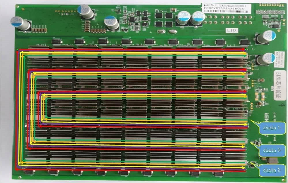
Fig 1. Signal Flow
Green line is CLK signal flow, chain0 is produced by Y5 25M crystal oscillator, transmits from No. 1-1 chip to No. 1-18 chip; chain 1 is produced by Y4 25M crystal oscillator, transmits from No. 2-1 chip to No. 2-18 chip; chain 2 is produced by Y6 25 M crystal oscillator, transmits from No. 3-1 chip to No. 3-18 chip; in standby and operation, voltage is 0.9V. Resistance is 780.
Orange line is TX (CI, CO) signal flow, IO Mouth Pin 7(TX2)/11(TX0)/17(TX1) in, transmits from No. 1 chip to No. 18 chip; the voltage is 0V when IO wire is not plugged, and the voltage is 1.8V in opearation. Resistance is 580.
Yellow line is RX (RI, RO) signal flow, returns from No. 18 chip to No. 1 chip, and then returns to control panel from IO mouth pin 8(RX2)/12(RX0)/18(RX1); the voltage is 1.8V when IO signaling wire is not plugged, and the voltage is also 1.8V in opearation. Resistance is 580.
Purple line is B (BI, BO) signal flow, lowers electrical level from No. 1 chip to No. 18 chip; the voltage is 0V when IO signaling wire is not plugged or in standby, and the singal impluse is about 0.3 in computing. Resistance 580.
Red line is RST signal flow, IO mouth pin 15(RST0)/21(RST1)/22(RST2) in, transmits from No. 1 chip to No, 18 chip; 0V when IO signaling wire is not plugged or in standby, and 1.8V in computing. Resistance is 440.
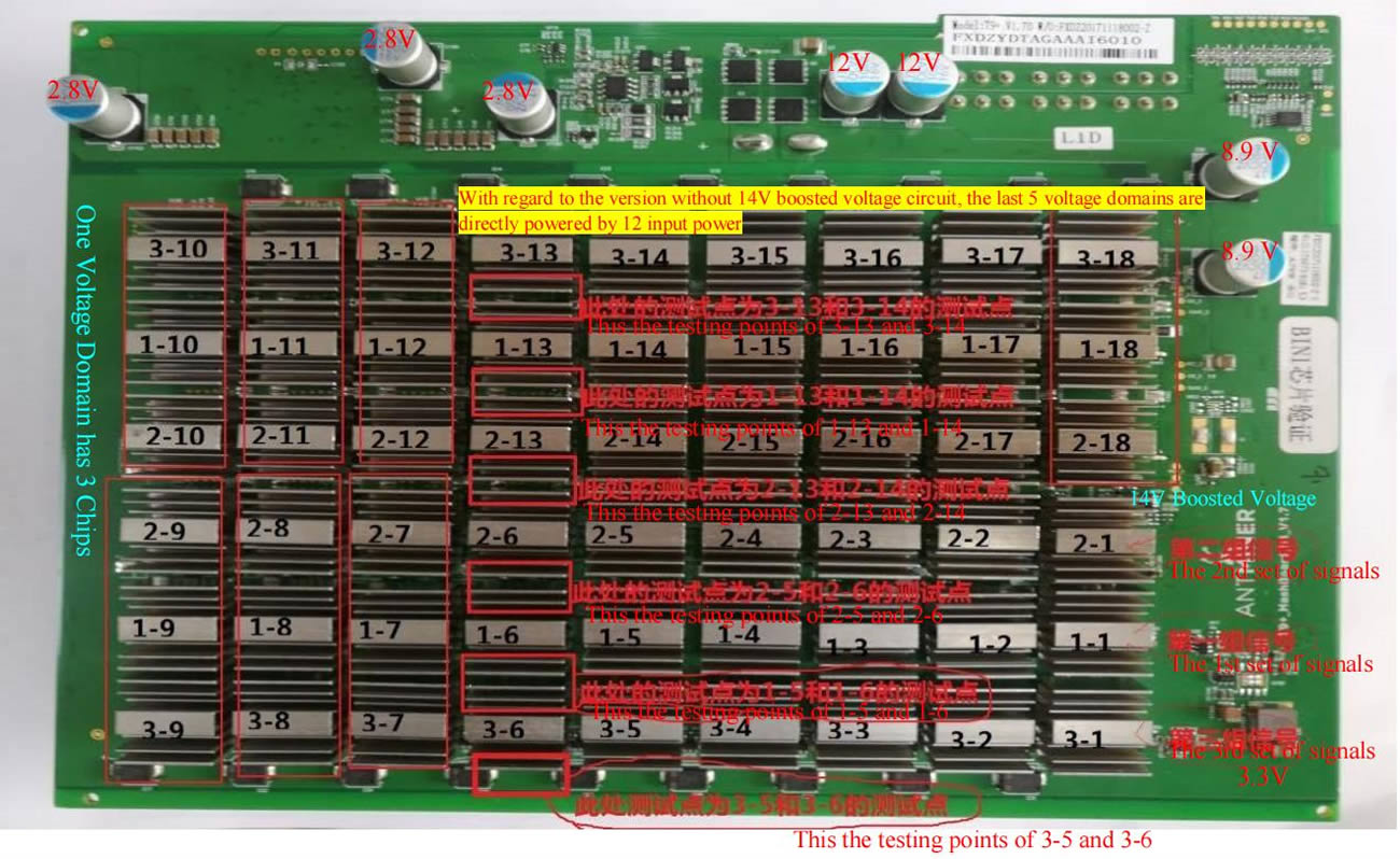
Fig 2
2. Fig 4 is the critical circuits on the front of T9+ Hash board.
1) Testing points among chips (as below fig 3 after amplification)
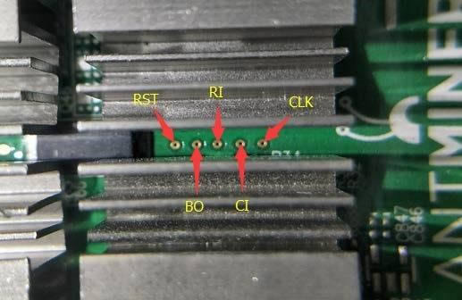
Fig 3. Testing Points among Chips
In maintenance, the most direct fault-locating method is to test the testing points among chips. The testing point arrangement of T9+ Hash board is as the following:
The sequence of the 9 voltages domains of the lower row: RST, BO, RI(RX), CO(TX), CLK.
The sequence of the 9 voltage domains of the upper row is reverse: CLK, CO(TX), RI(RX), BO, RST.
In maintenance, the right marks are the positions of testing points of lower row
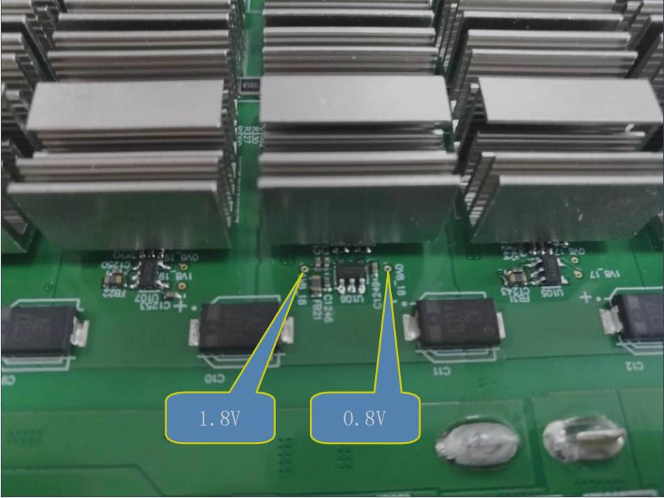
In maintenance, the left marks are the positions of testing points of upper row
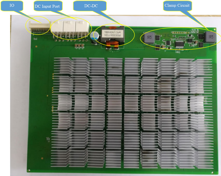
Fig 4. The Critical Circuits of T9+ Hash board
2) Voltage Domain: the entire board has 18 voltage domains, and each domain has 3 chips. The 3 chips in the same voltage domain are in associated.
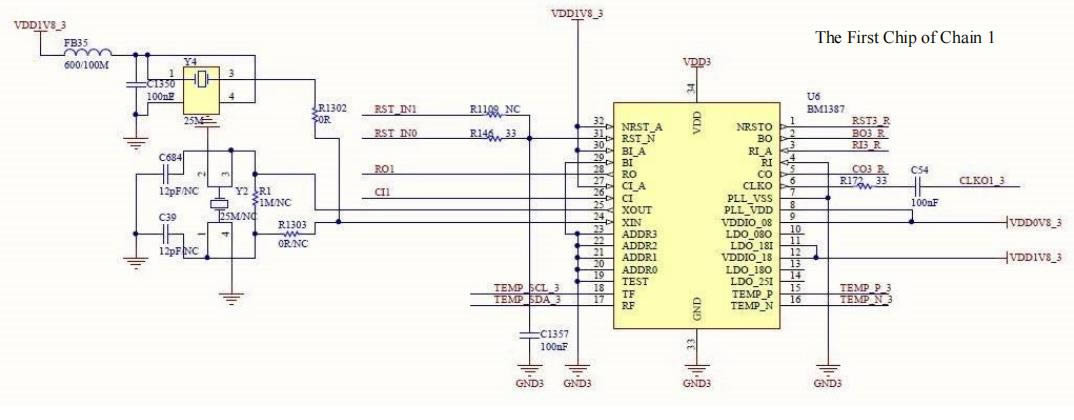
Fig 5. The Critical Circuits on the Front of T9+ Hash board
3) T9+ IO mouth TX Input and RX Output Circuits
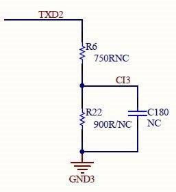
Fig 6. TX Input Circuit

Fig 7. RX Output Circuit
4) 14V Boosted Circuit (some versions have no circuit of this part) as Fig 8:
The responsibility is to boost DC-DC (8.3 - 9.2V) to 14V, and the principle is to boost 9V to 14V through U110 RT8537 switching power supply, the switching signal produced by U110 stores energy via L1 inductance, and then D100 boosted rectifying diode charges and discharges C954, and thereby get the 14V of C954 positive electrode.
The input voltage of external LDO of the last 5 voltages domains of T9+ V1.0, V1.1 is powered by 14 DC-DC booster voltage, and that of V1.2, V1.4, V1.5 is powered by the input 12V of single board.
Note: the abnormal rise of the voltage of boosted circuit often causes the LDO damage of the last 5 voltage domains of Hash board, and also causes chip damage easily. And the anomaly of boost voltage is often caused by the oxidation of U110, R812 and R811.
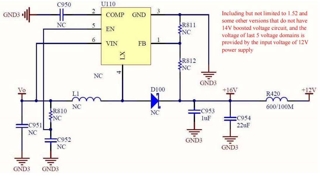
Fig 8. 14V Boosted Voltage Circuit
5) Principle Analysis of Voltage Domain Single Chip (see below Fig 9 and Fig 10):
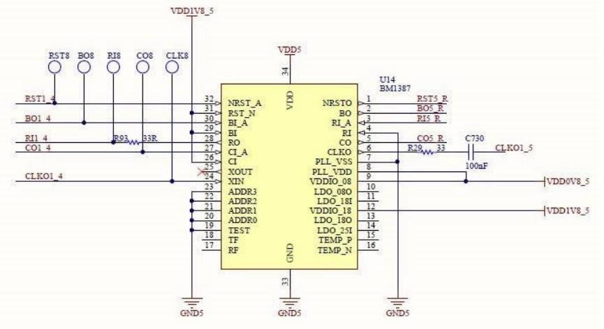
Fig 9. BM1387 Circuit Diagram
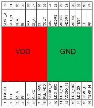
Fig 10. BM1387 Chip Pins
Signal Description
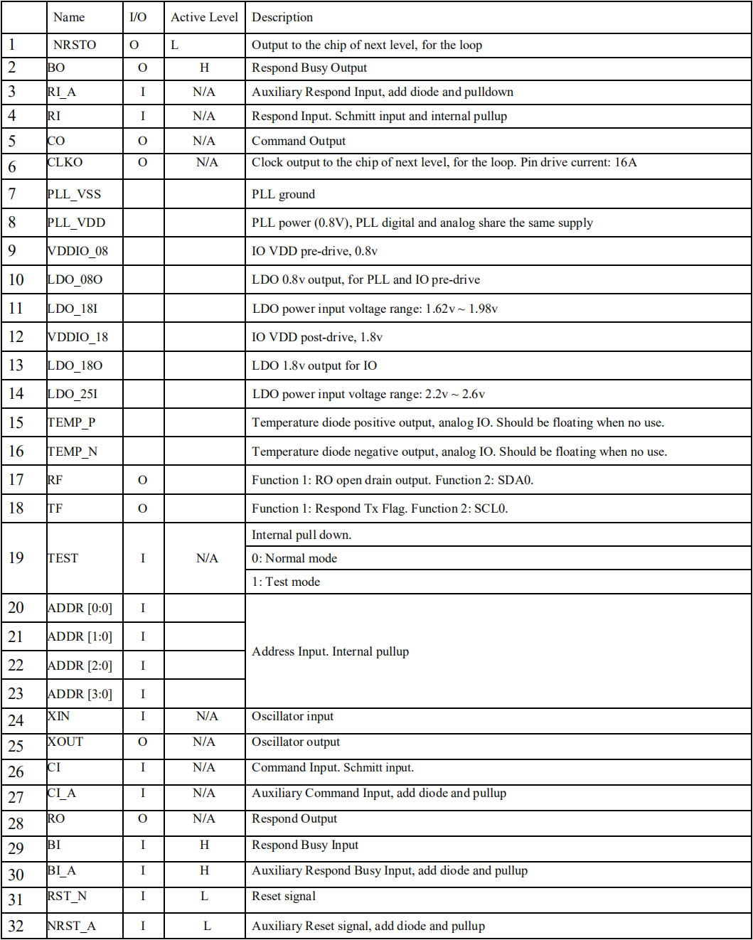
● The above is the pin functions of BM1387 chip.
In maintenance, mainly test the ten testing points on the front and back of chip (front and back have 5 respectively: CLK, CO, RI, BO, RST); CORE voltage; LDO-1.8V, PLL-0.8V; DC-DC output, and booster voltage 14V.
Test Methods:
1) When IO wire is not plugged and only 12V is plugged: DC-DC output is 0V or so, and booster voltage output is about 0V. PIC power supply 3.3Vmust be powered up. Other test voltages are all about 0;
2) When IO wire is plugged but test key is not pressed, DC-DC and booster voltage have no voltage output; when tool test key is pressed, PIC begins to work. At that moment, DC-DC outputs the voltage set up by PIC tool test program, booster voltage begins to work. Then tool outputs WORK and returns NONC after computing. This moment the normal voltage of each testing point should be:
CLK: 0.9V
CO: 1.6-1.8V. When tool just sends WORK, CO is negative polarity, so DC level will be lowered and the transient voltage is about 1.5V.
RI: 1.6-1.8V. In computing, anomaly voltage or low voltage will cause Hash board anomaly or zero hash rate. BO: 0V when there is no computing; and 0.1-0.3V impulse beat in computing.
RST: 1.8V. Every time when pressing tool test key, output reset signal again.
When any testing point status or voltage is abnormal, infer fault point according to the signal flow of testing point.
● It can be seen from above list:
CLK signal: Pin 24 in, Pin 6 out, when crossing domains, Pin 6 out, via a 100NF capacitor, enters the Pin 24 of the next chip.
TX signal: Pin 27 in, Pin 5 out;
RX signal: Pin 4 returns, Pin 28 out;
BO signal: Pin 30 in, Pin 2 out;
RST signal: Pin 32 in, Pin 1 out.
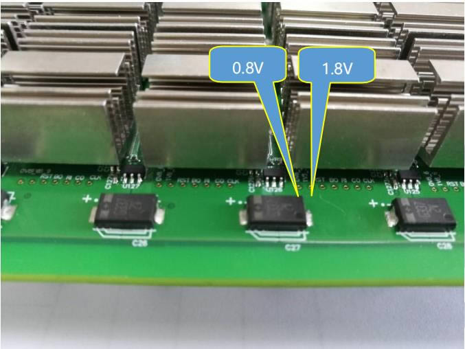
As shown in below Fig. 10: it is able detect each signal voltage of chip, including CORE voltage, LDO-1.8O, LDO-1.8I, PLL-0.8, LDO- 2.5I, etc.
CORE: 0.45V — generally the chip CORE short circuit of this voltage domain will cause this voltage anomaly.
LDO-1.8: 1.8V — LDO-1.8 short circuit or open circuit of this chip will cause this voltage anomaly.
PLL-0.8: 0.8V — PLL-08 power supply short circuit of a chip of this voltage domain or LDO-1.8 anomaly will cause this voltage anomaly.
3) Determine the operation status of Hash board, hash rate of chip, temperature sensing, etc. according to print window information of test tool.
3. IO Mouth: IO is composed of 2×12 pitch 2.0 PHSD 90°in -line double row. The definition of each pin as below Fig 11:

Fig 11. Each Pin Definition of IO Mouth
As shown in above Fig:
Pin 1, 2, 9, 10, 13, 14, 19, 20, 23, 24: GND.
Pin 3 and 4 (SDA, SCL): the I2C bus wire of DC-DC PIC, connect control panel to communicate with PIC; through which control panel can read and write PIC data, and thereby control the power supply voltage of Hash board.
Pin 5 (PLUG0): the identification signal of Hash board, this signal raises 10K resistance to 3.3 V by Hash board, so this pin is high level 3V when IO signal is plugged.
Pin 11, 12 (TXD0, RXD0), Pin 17, 18 (TXD1, RXD1), Pin 21, 22 (TXD2, RXD2): hash rate channel of
Hash board 3.3 end, and changes into TX (CO), RX (RI) signals through resistive voltage division; the electrical level of all IO mouth pin ends is 3.3V, and changes into 1.8V through resistive voltage division.
Pin 15 (RST0), pin 21(RST1), pin 22 (RST2): reset signal 3.3V end, and changes into 1.8V RST reset signal through resistive voltage division.
Pin 6, 16 (ID): ID identification pin of Hash board, mainly providing control panel with Hash board
ID. Below Fig 12 shows each pin of IO
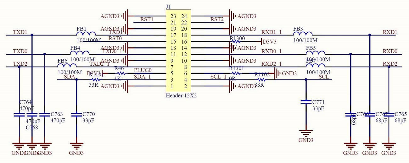
Fig 12. IO Signal
4. 3.3V Reduction Voltage Circuit: 3.3V power supply for Hash board, mainly providing PIC and EPROM with working voltage.
Responsible for reducing voltage to 3.3V from 12V, and the principle is to reduce 12V to 3.3V through U115 MP1484 switching power supply, the switching signal produced by U150 stores energy via L30 inductance, charges and discharges C1345, gives sampling feedbacks via R1202/R1203 to U150 and thereby controls the voltage of C1345 positive electrode. See Fig 14 and Fig 15:
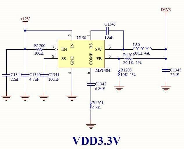
Fig 14. 3.3V Reduction Voltage Schematic
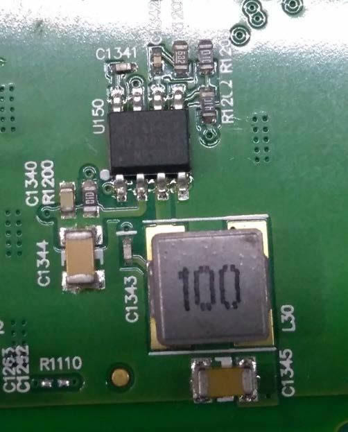
Fig 15. 3.3V Reduction Voltage PCB
5. DC-PIC: Composed of PIC133EP16 chip and EPROM chip AT24C02. See Fig 16 and Fig 17:
PIC controls the device in relation to chip frequency information of Hash board and voltage value, through which we can control the DC-DC output voltage of Hash board.
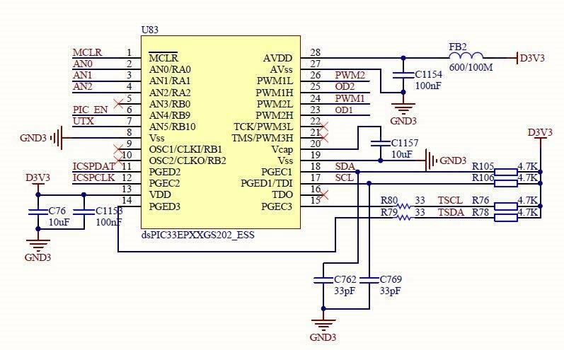
Fig 16. PIC Schematic Diagram
When PIC works, it needs to control and send a heartbeat signal every 10 seconds or so. Without heartbeat information, PIC will be closed after 10 seconds. PIC pin 13 is VDD 3.3V, pin 8 is GND, pin 11 and 12 are I²C bus wire that connects IO mouth to control panel, pin 2, 3 and 4 are PIC addresses; pin 4 is PIC 3.3V; pin 24 and 26 are the PWM output of PIC, pin 23 and 25 are the OD output of PIC, and control DC-DC voltage; pin 6 is EN signal that PIC outputs, and controls DC-DC operational status.
EPROM stores information covering chip frequency information, voltage value, etc. Every time before working, PIC firstly read data like computing frequency of Hash board, voltage, etc. of last time from EPROM.
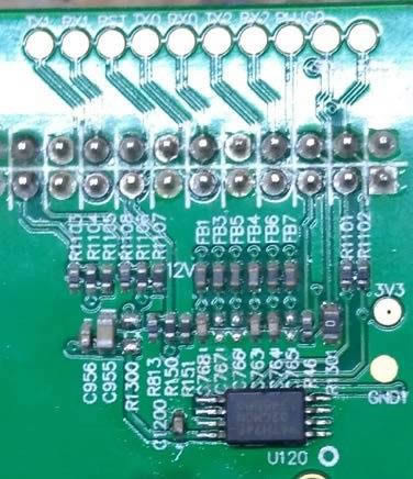
Fig 17. EPROM Locality Map
EPROM stores the information like voltage, frequency, etc. of T9+ Hash board, and Fig 19 is EPROM Schematic
6. DC-DC Circuit: Parallel clamping circuit composed of MAX15026 and CMOS tube TPHR9003NL as well as MBR0540 and NCP3420D. See Fig 18 and Fig 19
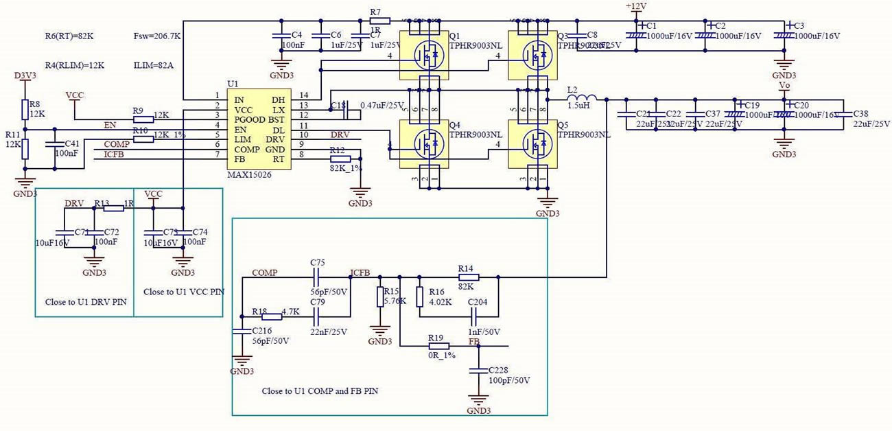
Fig 18. DC-DC Schematic Diagram
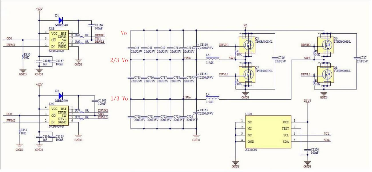
Fig 19. Clamping Circuit Schematic Diagram
MAX15026 voltage regulator produces PWM switching signal to drive the two pairs of MOS tubes (Q1/Q3, Q4/Q5) of upper and lower bridges, and stores energy via L2 inductance, NCP3420D, driven by PIC, produces PWM switching signal to drive the two pairs of MOS tubes (Q2/Q7, Q6/Q8) of upper and lower bridges, and then filters via C19 and C20 after connection.
MAX15026 main function pins:
Pin 1: 12 V power supply
Pin 9: GND
Pin 4: EN control, connect PIC pin 6, and control the operational status of DC-DC circuit via PIC Pin 7: FB feedback, connect VO via R14
Pin 2: VCC
Pin 13: bootstrap capacitor 10V+ Pin 12: switching signal
Pin 11: lower bridge drive Pin 14: upper bridge drive
When the voltage of DC-DC is abnormal, firstly check the consistency of voltage value of PIC and DC-DC output voltage through tool print information; if they are inconsistent, replace the low capacitance aroundLM27402SQ;
If DC-DC has no output, check whether L4/L5 loses material oris burned-out; if L4 loses material, check Q6, Q8 and U90 again to find whether they are damaged; if L5 loses material or is burned-out, check Q2, Q7 and U88 again to find whether they are damaged; try to measure out all damaged materials at a time, and replace them materials at a time, in case that there are still poor materials which might burn out new materials again due to the replacement of part of materials.
7. 25M CLK: Composed of Y 25MHZ passive crystal oscillator and 100nF: See Fig 20 and Fig 21.
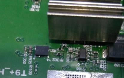
Fig 20. 25M CLK Circuit
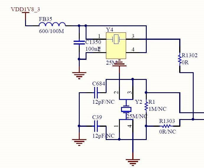
Fig 21. 25M CLK Schematic
8. 1.8V-LDO: Composed of 1.8VLDO SPX5205M5_L_1_8.
See below Fig 22 and Fig 23:
SPX5205M5 pin 1 and 3 in, pin 5 1.8V out;
Note: the LDO power supply of T9+ Hash board has two types. The first type is that every voltage domain of Hashboard has an external LDO SPX5205M5, responsible for the LOD of the 3 chips of each voltage domain; the other type is that only the last 5 voltage domains have external LDO, and other voltages are powered by chip built-in LDO; all BM1387 chips have built-in LDO power supply circuit, BM1387 pin 14 (LDO-25I) in, pin 12(LDO-18O) out, and each chip has independent LDO without mutual interference. The LDO-25I power supply of the last 5 voltage domains are from 14V boosted circuit; and the LDO-25I of other voltage domains are from chip itself.
PLL-08 voltage is from LOD-1.8 via voltage division of two resistances.
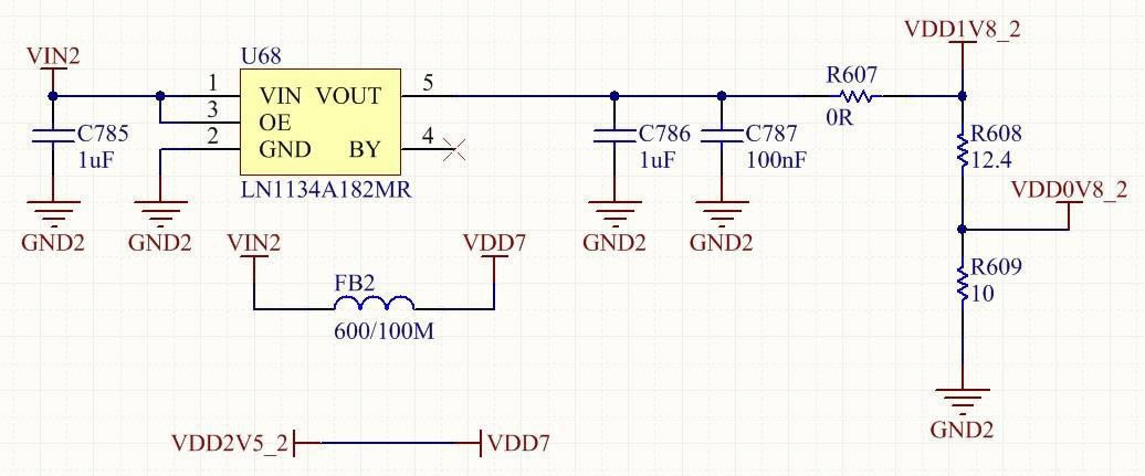
Fig 22. 1.8V Voltage Stabilizing Circuit
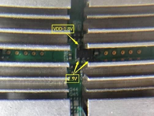
Fig 23. 1.8V Voltage Stabilizing Circuit
9. Temperature sensor circuit: two temperature sensors, one is TEMP (PCB), consisting of sensor IC; the other is TEMP (CHIP), and this is composed of chip build-in temperature sensor (BM1387 pin 2 and pin 16). These two temperature sensors collect parameter, and return to FPGA of control panel from RI via BM1387 pin 17 and pin 18. The principle is as Fig 24:
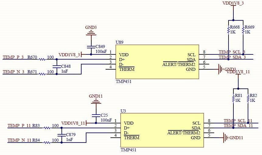
Fig 24. Temperature Sensor Schematic Diagram
T9+ Temperature Sensor IC connects the first chip (U6) of No. 2 signal chain
IV. The Troubleshooting of T9+ Single Board
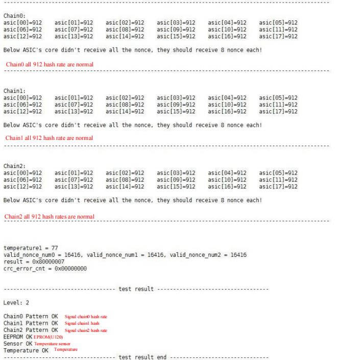
Test Results of Normal miner
1: Report 0 or numeral
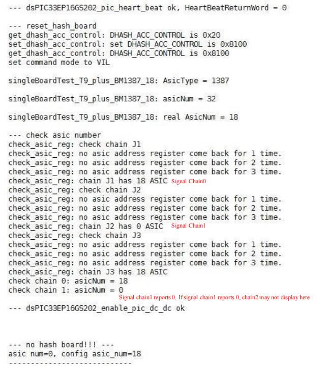
Maintenance method refers to the report of 0 situation of S9. Note: the 3 chips in 1 voltage domain belong to 3 signal chains. If one chip has problem or is not installed properly, it will affect the other two signal chains. For instance, the fault has been located in above Fig. Improper installation of the chip might cause that three signal chains report 0 together.
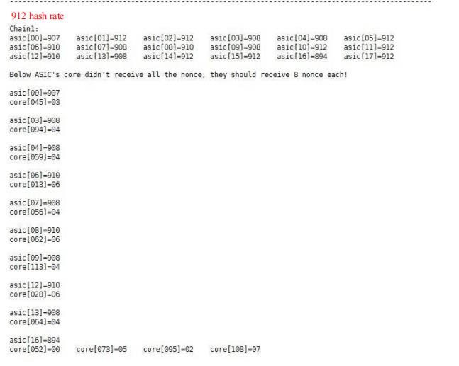
2: low hashing:
Maintenance method refers to the low hashing situation of S9.
Note: Low hashing of T9+ will cause spam and auto reboot.
V. Troubleshooting of Complete miner
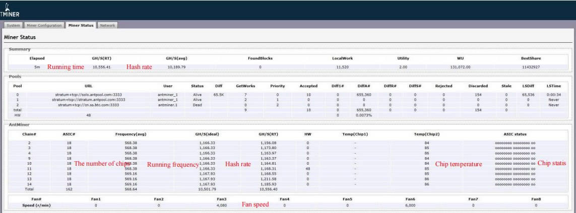 Test Results of Normal miner
The fault standard and troubleshooting of T9+ complete miner test refer to S9.
a. Hash board of T9+ is displayed as 3 boards on the background web page.
b. 9 and 10 belong to the first Hash board, 3, 11 and 12 belong to the second Hash board, and 4, 13 and 14 belong to the third Hash board. When which three boards belong to one Hash board can not easily determined, see the temperature behind. The three boards with same temperature belong to one Hash board. For most miners, the temperatures of the three Hash boards are different.
VI. Maintenance Process
● sample:

1. Regular Check: observe the target board to find cooling fin displacement, deformation or burn? Such issues take priority, displacement can be solved by taking it off, wash off the glue and re-glue it after the maintenance. If there is no problem, then check impedance of each and every voltage domain to see if there is short/open circuit, which then takes priority. Check if every domain reaches 0.45V and voltage different no greater than 0.05. Voltage too high or too low suggests anomalies in the neighboring domains.
2. After regular check (in which short circuit check is a must, in case of burning chips or other fittings when power is on), check the chip with hash board tester, judge and pinpoint based on such result.
3. Based on hash board tester results, check test point from the malfunctioning chip, (CLK IN OUT/TX IN OUT/RX IN OUT/B IN OUT/RST IN OUT), and VDD VDD0V8 VDD1V8 VDD2V5.
4. Signal flow, apart from RX (No.63 to No.1), are sequential (CLK C0 B0 RST) from No.1 to No.18. So the anomaly can be identified with power sequence.
5. When pinpointed the malfunctioning chip, re-solder the chip: add scaling powder around the chip, heat the chip pin to dissolved state, move and press the chip lightly; have the chip pins and soldering pans re-grinded, finish. Note that if re-soldering does not help, the chip should be changed directly.
6. Run at least twice with hash board tester on fixed Hash board. Test timing: first time should be after changing fittings, with cooled board. The second time should be in a few minutes with fully-cooled board. The gap between two tests will not affect working. Put aside the repaired board and continue with another one, come back to the first one with the fixed second one
7. Log the malfunction type after maintenance, esp. the model, location and reason. This will further improve the feedback to production, CS and R&D.
8. Conduct formal burn-in after logging.
VII. Malfunction Types
Typical malfunctions of T9+:
1. Missing cooling fin or cooling fin displacement/deformation: No cooling fin displacement or touch on the PCB (back side of the board) before power-on, esp. fins in different voltages. Fins of different voltage domains touching will result in possible short circuits. Make sure all fins are in good condition of heat-transitioning and fixed tight. Before replacing or re-implanting fins, clean the residue on the fin and the board first. Residue can be handled with anhydrous alcohol.
2. Imbalanced impedance among multiple voltage domains: When the impedance of certain domains is deviated from the norm, the anomaly domains could comprise open/short circuits. It is most likely that the chips are the cause. But there are 3 chips in each voltage domain; the problem could be with only one of them. Check and compare the earth impedance of each test point on chips to find the anomaly point and thus locating the problem chip.
Short Circuit: remove the cooling fin from the chips in the same voltage domain and observe chip pin to spot bridging issue. If you cannot find short circuit point by observing, find it by resistivity method or interception method.
3. Imbalanced voltage among domains: Voltage too high or too low suggests IO signal malfunction in the anomaly domain or the neighboring domain. This cause the next domain to show abnormal status and then: voltage imbalance. Check the signals and voltages in test points to find the anomaly point. Some of the cases may require you to compare the impedance among multiple test points to find the anomaly.
Pay special attention: CLK signal and RST signal — anomalies of these 2 are most frequently causing voltage imbalance.
4. Missing chips: Missing chips means that when conducting hash board tester checks, all 18 chips (three chains display respectively) cannot be found, but only some of them. The actually missing (cannot find by checking) anomaly chips are not in the shown location. You need to pinpoint the anomaly chip by testing. The pinpointing can be conducted by intercepting TX. Pivot the TX signal of a certain chip over the land, such as, after setting the TX output of chip No. 14, over the earth and all previous chips are normal, the hash board tester should show 50 chips. If not, the anomaly exists before No. 14; if it does, the anomaly chip is after No. 14. Repeat this until you locate the anomaly chip bydichotomy.
5. Broken link: Broken links are similar to missing chips. The difference is that not all missing chips are in anomaly, but only one abnormal chip causing the following chips to fail. Such as, a certain chip is functional, but it does not transmit information from other chips; this signal chain will be broken right here — this is called broken link.
Hash board tester is capable of showing broken links. Such as when checking chips, hash board tester reports only 14 chips; hash board tester cannot start running until it detects pre-set number of chips, so it only shows the number of chips found. Based on the number “14”, check the voltage and impedance at test points right before and after chip No. 14 will help you to locate the problem.
6. No running:
No running means the hashboard tester cannot detect the chip information of the Hash board and shows “No hash board”; this is the most frequent problem.
1) Voltage anomaly of a certain voltage domain: check the voltages among multiple domains to locate the problem.
2) Chip anomaly: Check signals among test points to locate the anomaly.
CLK signal: 0.9V; signal is from chip No. 00 to No. 17. But the current edition offers only 1 crystal oscillator, abnormal CLK causes all subsequent signals to show anomaly. Find the target in the sequence of signal transmission.
TX signal: 1.8V; this signal is from chip No.00, 01...17, look for previous ones when you hit anomaly at a certain point.
RX signal: 1.8V; this signal return from 17...01, 00, identify the malfunction reason by checking signal direction. When no running happens to Hash board, this signal takes priority, check it first.
BO signal: 0V; this signal means that when the chip detects RI return signal in a normal state, it can be set down to low level, otherwise it should be high level.
RST signal: 1.8V; when the board is powered on and plunged in IO signal, this signal will transmit from 00, 01…17 and till the last chip.
3) Caused by a certain chip
Check the PD among multiple domains. In normal conditions, the VDD voltage is 0.45V, all the voltages on other test points should be 0.4V5 as well, a balance among multiple domains is necessary.
4) VDD1V8 voltage anomaly of a certain chip
Check the test points of voltage domains to determine whether or not a certain VDD1V8 is normal. Generally, IO voltage determines the voltage of test points. Therefore, when the IO voltage is 1.8V, the test points have a normal voltage of 1.8V.
5) VDD2V5 anomaly of a certain chip
Make sure the voltage is normal. Abnormal voltage is related to low VDD voltage.
6) Buck and Booster Circuit Anomaly
Check the C8 capacitor output (up-left) and see if the voltage is between 8.27V and 9.07V. Those who are not in the scope may be in need of a re- upgrade to the U3 PIC; make sure the PIC voltage is normal, check to see if U100 has an output of 14V; also check the un-checked peripheral parts and U100 per se.
7. Low hashing:
Low hashing can be divided into:
1) Hash board tester shows NG due to insufficient Nonce and low hashing. The serial port shows information on the number of Nence each chip returns. Generally, if the Nence number is lower than the pre-set value, you should look for chip malfunction. If it is not due to poor soldering or peripheral reasons, you should just replace the chip.
2) Hash board tester shows normal status, but after installation the hashing is low. This is generally due to poor cooling of the chips. Pay special attention to the cooling fin glue, and the general ventilation. Another reason could be that the voltage of a certain chip is critical, and after installation, the 12V power supply is different from the test power supply, thus together resulting in a difference between test hashing and actual running hashing. Tune down and test with the hashboard tester, esp. with the DC adjustable 12V power supply. Find the voltage domain that returns the minimum number of Nence.
8. NG of a certain chip:
Means that when testing with hashboard tester, the port information shows the Nence is insufficient or zero of the return of a certain chip. If it’s not due to poor soldering or peripheral reasons, just replace the chip.
VIII. Maintenance Notes
1. The operator should be familiar with the function, flow direction, normal voltage and earth impedance values of each test point.
2. The operator should be familiar with chip soldering to avoid PCB blistering, deformation or pin damage.
3. BM1387 chip is packaged with 16 pins on both sides. Make sure of the polarity and coordinates when soldering.
4. When replacing the chip, clean all the heat-conducting glue on the chip to avoid IC poor soldering or poor cooling (which causes second-time chip damage)
Other Notes:
1. The Chip’s back side cooling fins are earth connected with the chip, so it is imperative to use a long slim electro probe to check the test points. The probe should be fully insulated with heat-shrink tubes other than the metal on the tip to avoid that the probe touching the cooling fin and the test points at the same time. The voltage difference between upper and lower circuits, so touching the earth of different domains (cooling fins) and test points could cause man-made damage to the chip. Please pay special attention.
2. Soldering. There are cooling fins right next to the PCB on the back side of the chip, thus the cooling is fast. So during soldering, you would need auxiliary heating at the bottom (about 200 degrees Celsius). This improves efficiency and reduces damage to the PCB. Without auxiliary heating device, you need to remove the cooling fins on the PCB on the back side of the chip first before replacing the chip.
عملاؤنا الكرام:
مرحباً! تبدأ عطلة عيد العمال الصيني من 1 إلى 5 مايو 2026 (بتوقيت غرينتش +8). سيتم تعليق خدمات الشحن الدولي خلال هذه العطلة. ستقوم شركتنا بتعليق الشحنات بعد ظهر يوم 30 أبريل 2026، وستُستأنف عمليات الشحن من المستودعات يوم 6 مايو (بتوقيت غرينتش +8). نعتذر بشدة عن أي إزعاج قد يسببه هذا الأمر. شكرًا لتفهمكم ودعمكم.
مع خالص التقدير،
ZEUS MINING CO., LTD.